
proj5
5.1
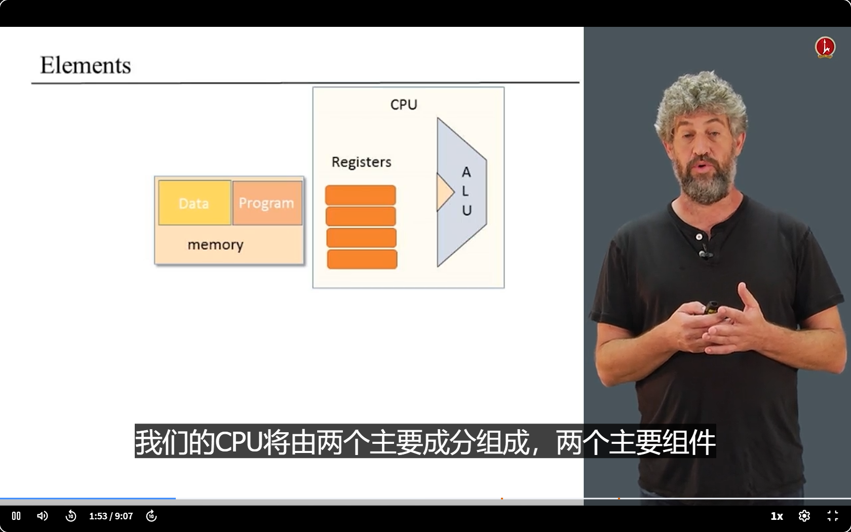
Elements
Infomation Flows
Element + 三条总线
(大概看看,具体的看后面)
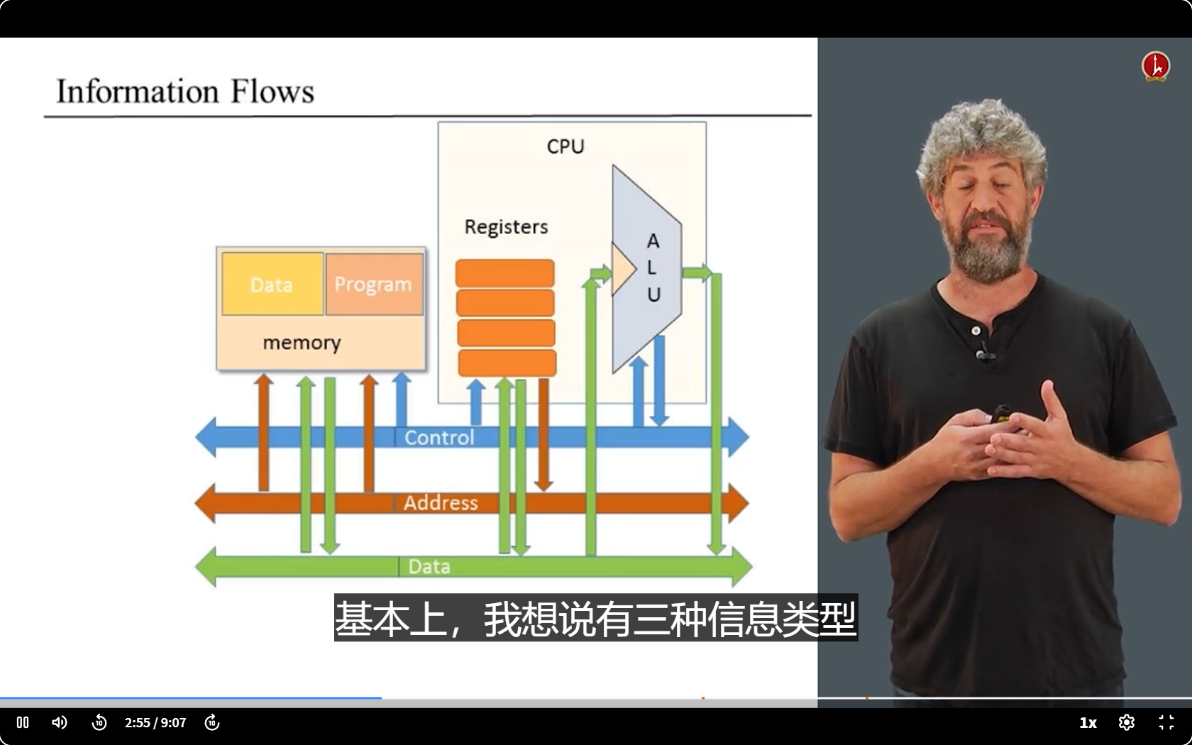
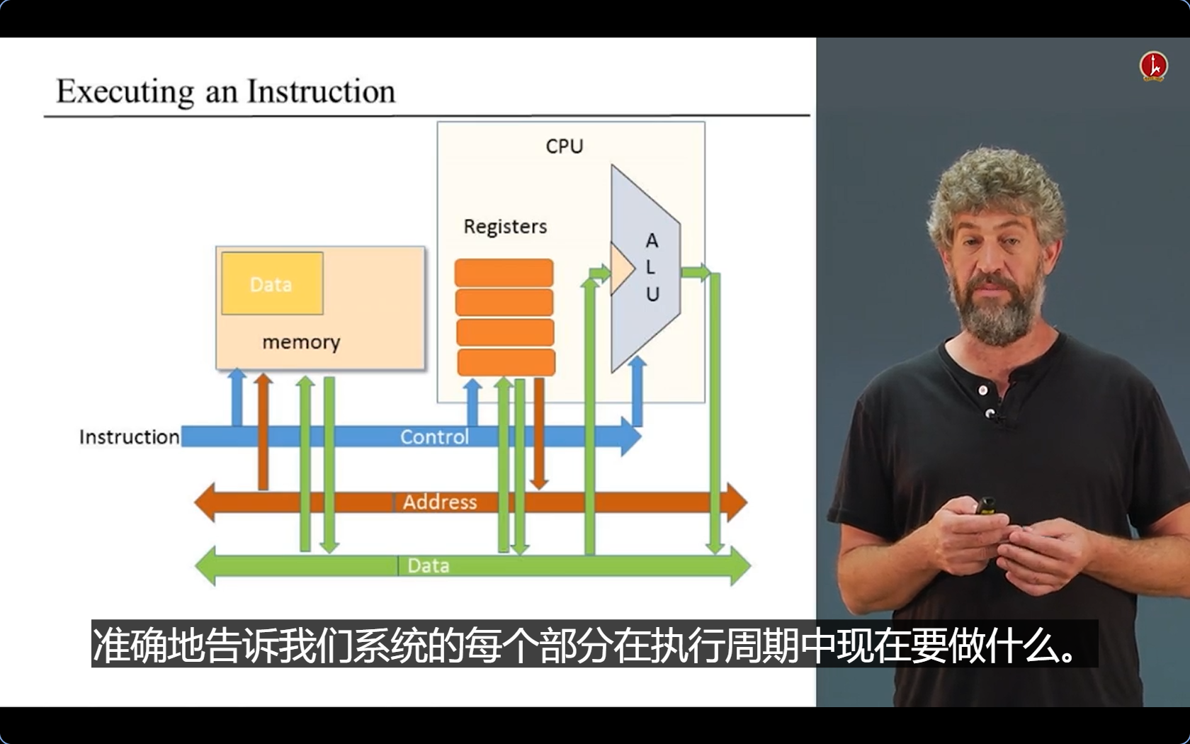
The Arithmetic Logic Unit
- data接入ALU,得到输出
- 输出值返回数据总线
- 我觉得是输出out或者回去内存?
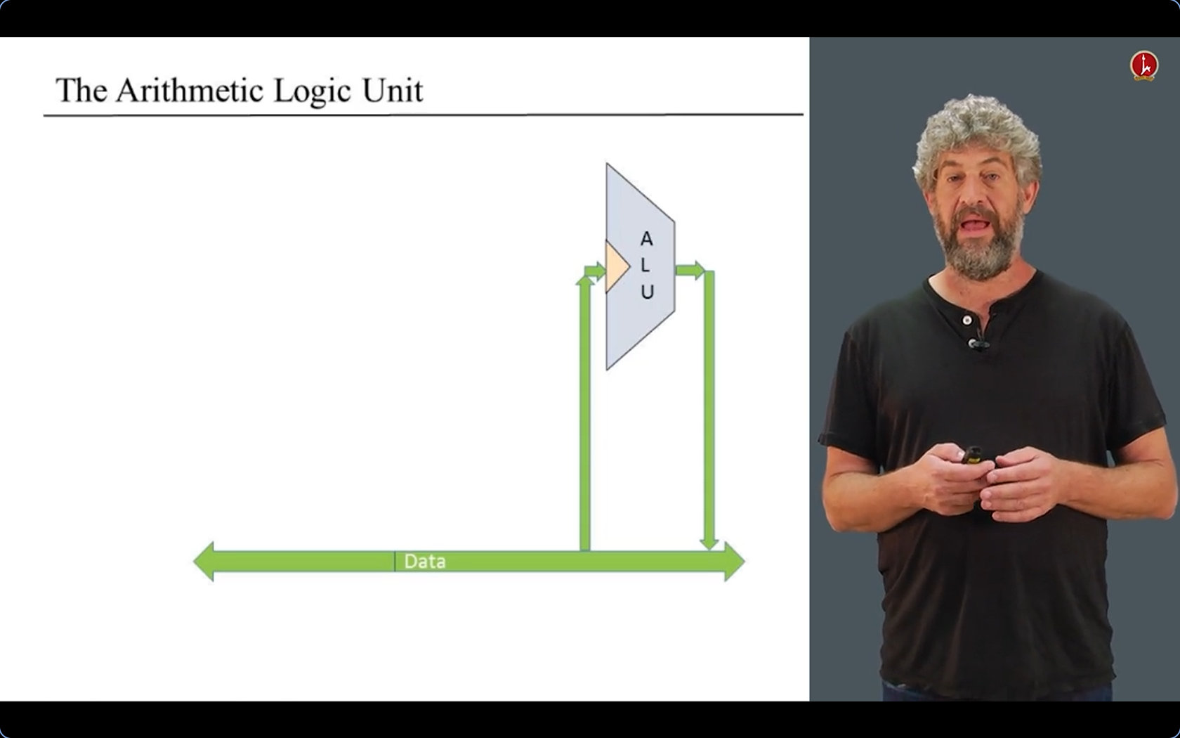
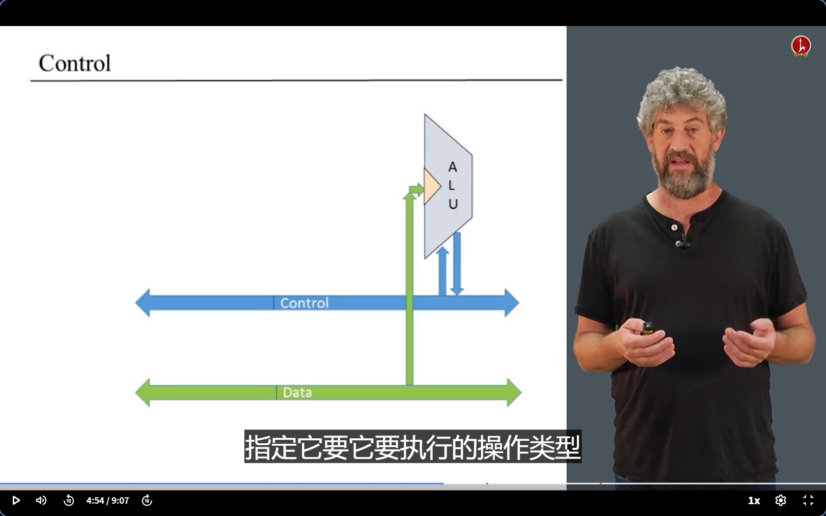
- control总线 告诉ALU进行何种操作
- ALU 返回告诉 Control 系统其他部分进行什么操作
- 当 CPU 从程序内存中获取到指令后,会对指令进行解析。对于指令中的控制信息,通过控制总线传出去(让算术逻辑单元、寄存器、内存等部件按要求操作,比如让算术逻辑单元进行加法运算等)
- 例如如果ALU发现某个数字大于零,他将告诉Control下一个指令的跳转以及下一个指令是什么
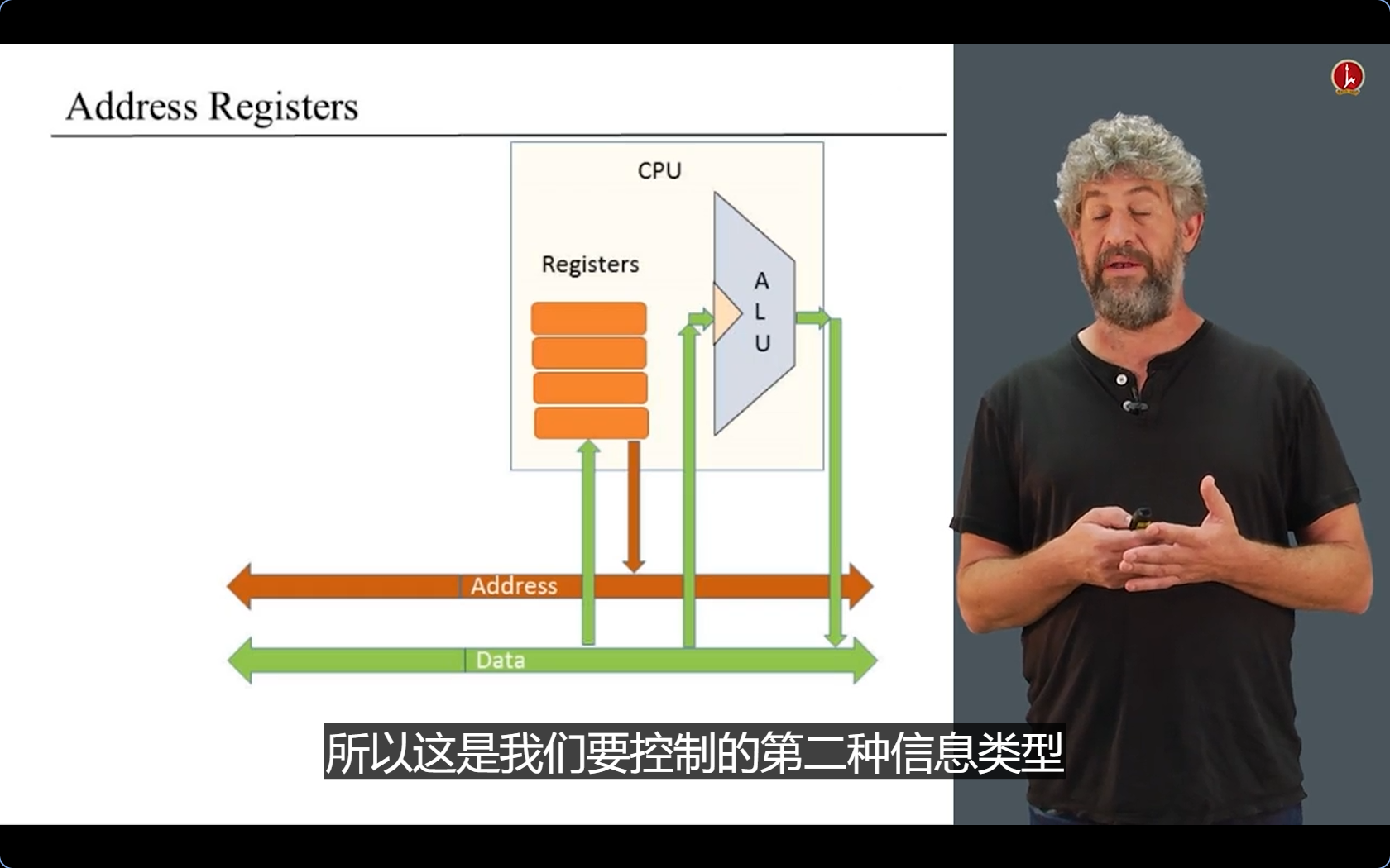
Address Register
- 寄存器储存中间结果。所以数据总线接到Register里
- 有的寄存器还用作地址储存器,所以register要接入地址总线
- (将数字,也就是地址放入寄存器中,然后它就指定了我们想要访问的位置。)
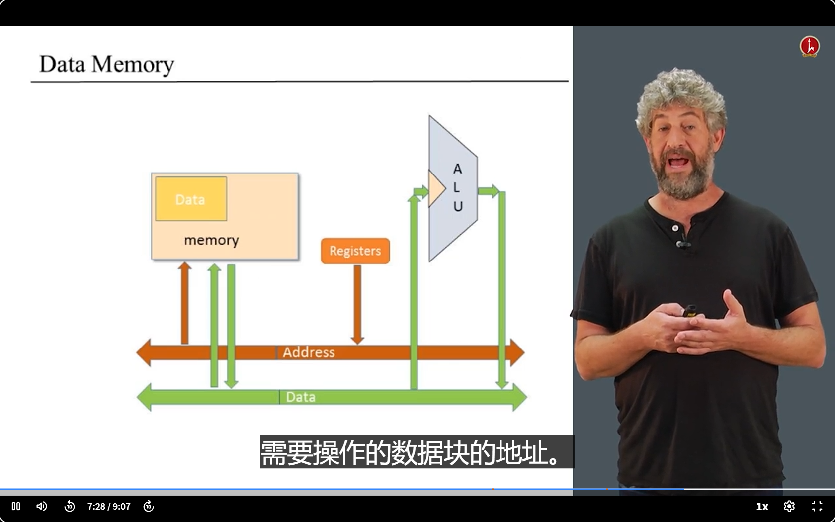
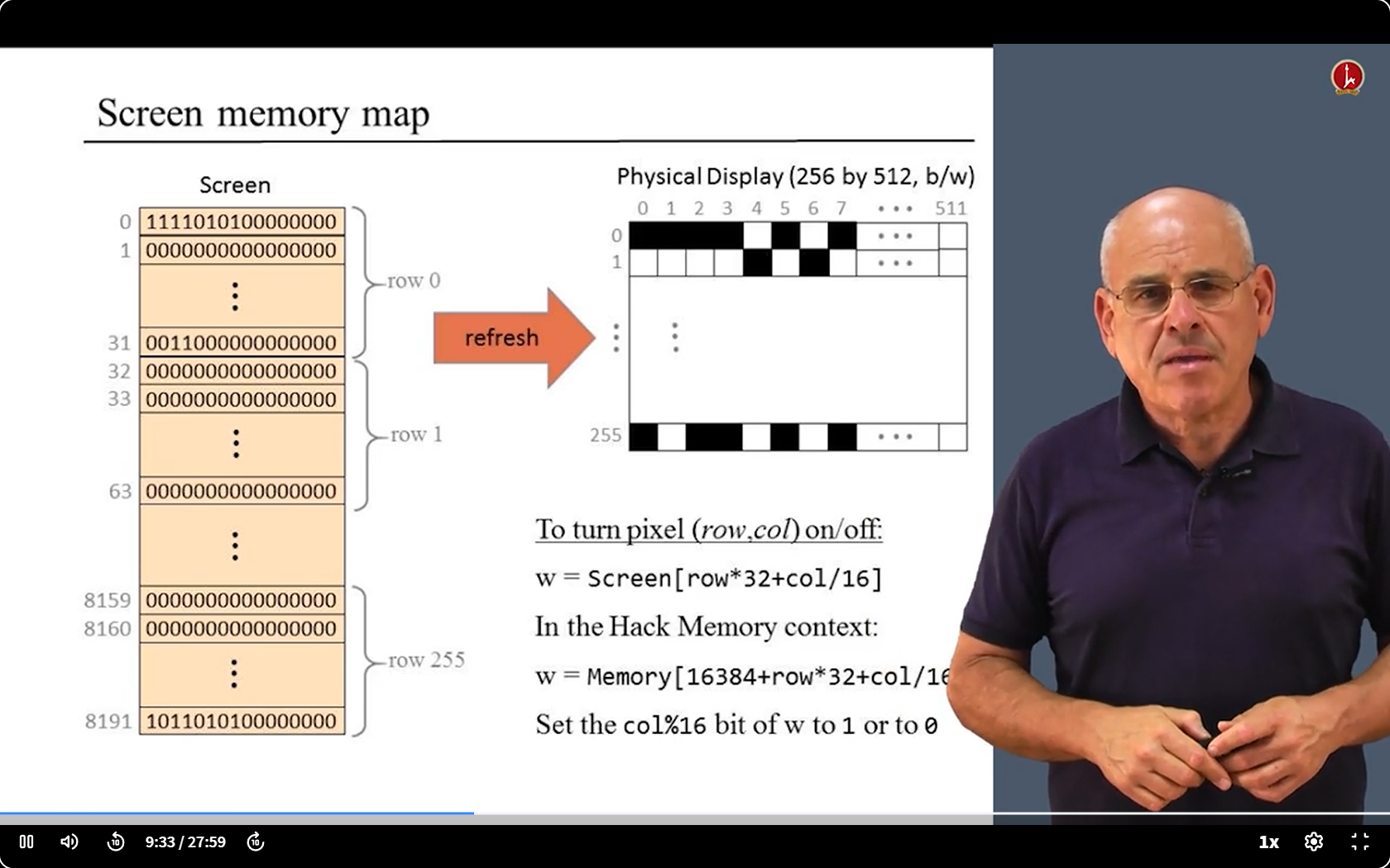
Memory
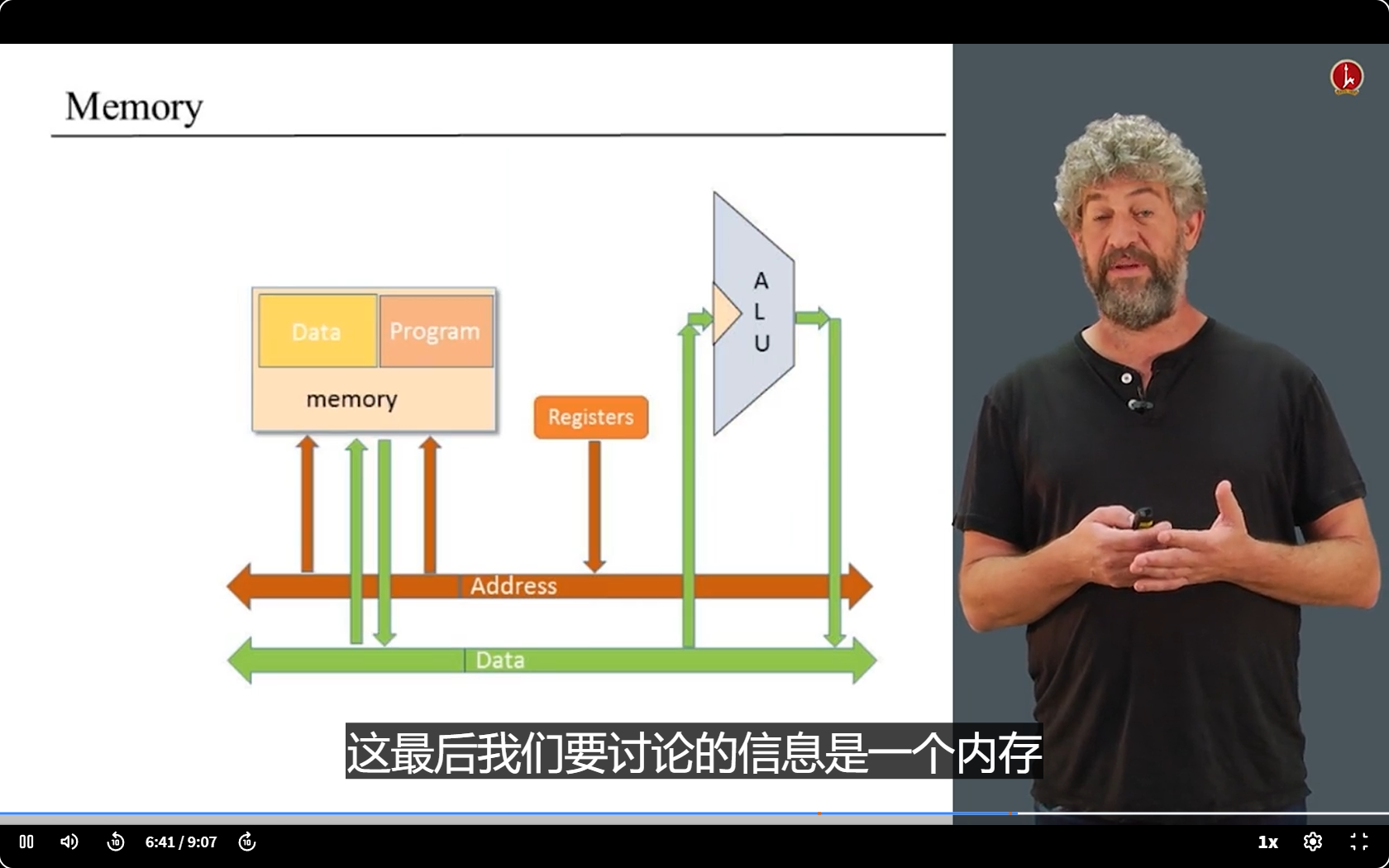
Data Memory
- Data Memory需要连接数据总线:因为输入和输出(这没问题)
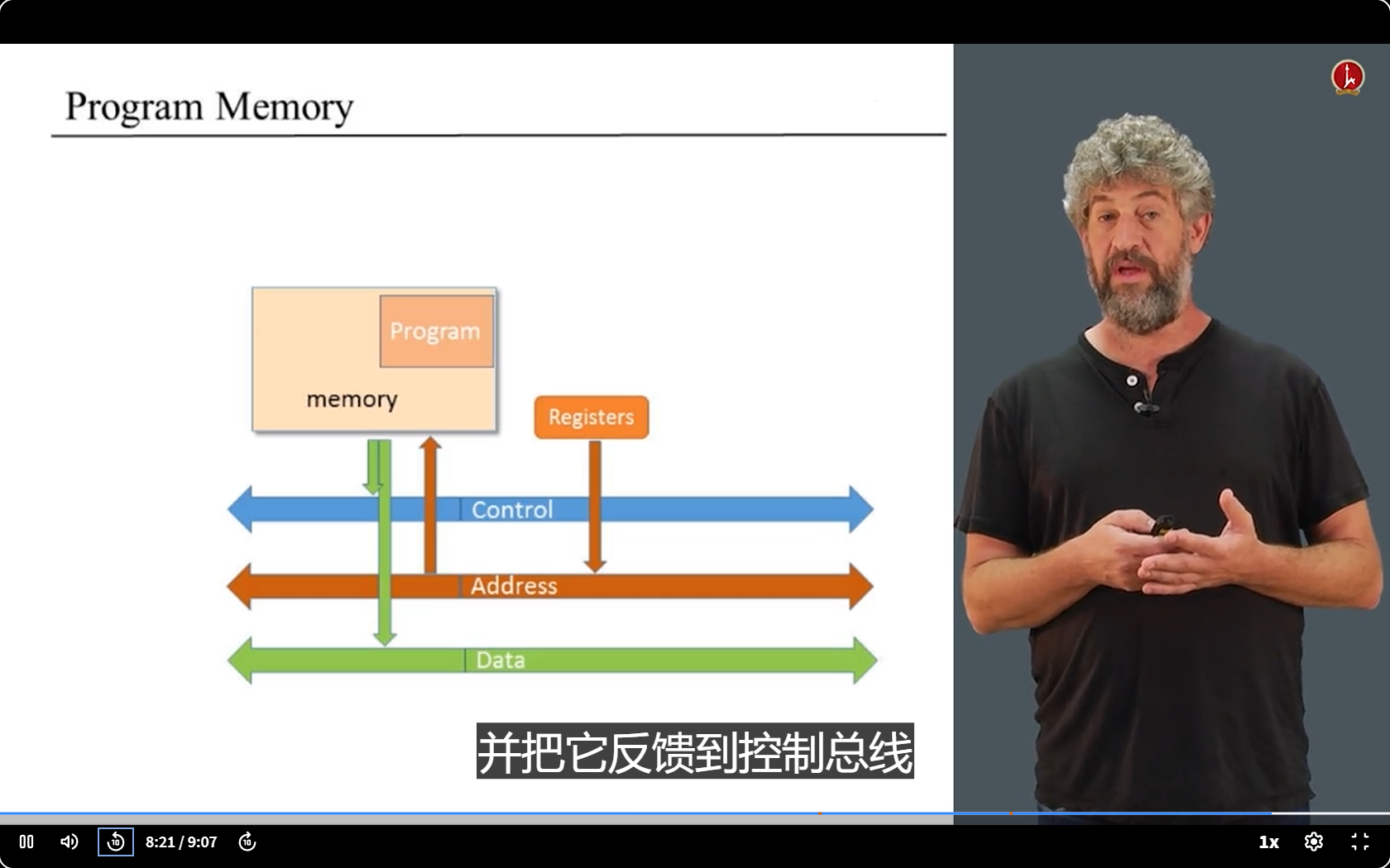
Program Memory
- 程序内存
- 需要从PM取出CPU所需要的程序指令,所以连接地址总线
- 例如,(程序指令是 CPU 找内存要的),CPU 要从程序内存里拿指令时,得先把下一条指令的地址发出去(通过地址总线),程序内存收到地址后,按地址找到指令再传给 CPU(通过数据总线)。
Next
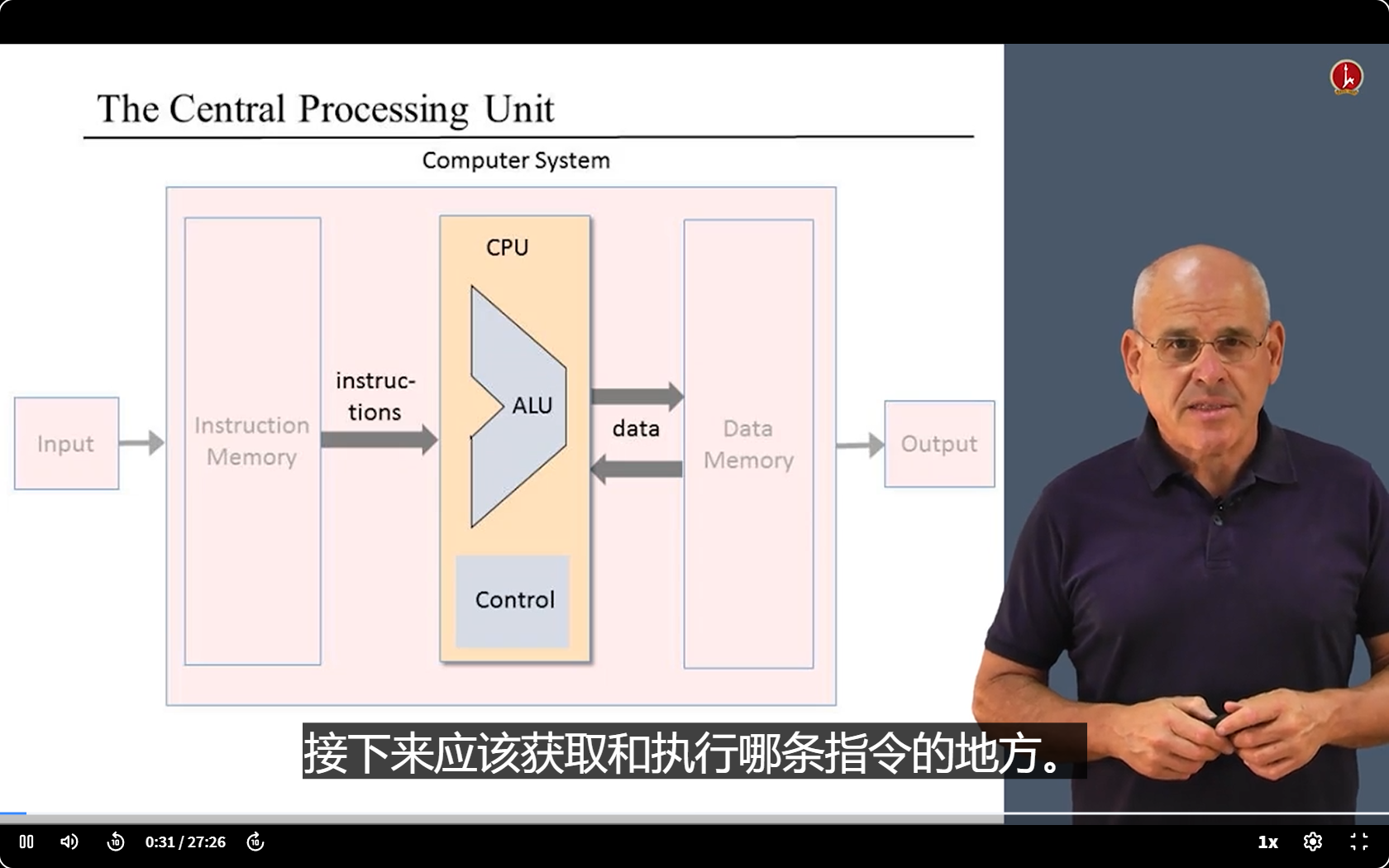
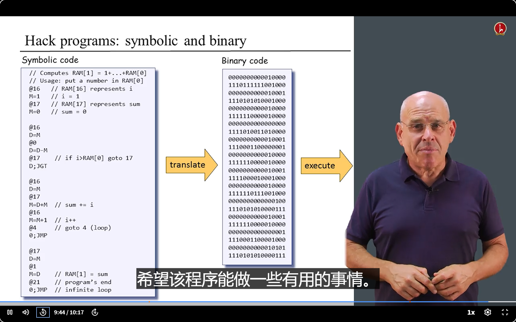
我们在下一单元要做的,是更仔细地研究最内层的循环,也就是我们的硬件应该执行的基本操作:即从内存,程序内存中取出一条指令,并恰当地使用系统的其他部分来执行它。这被称为取指 - 执行周期,这将是下一单元的内容。(一条一条执行程序指令)
5.2 The Fetch-Execute Cycle
The basic CPU loop
一条条 获取-执行 程序指令
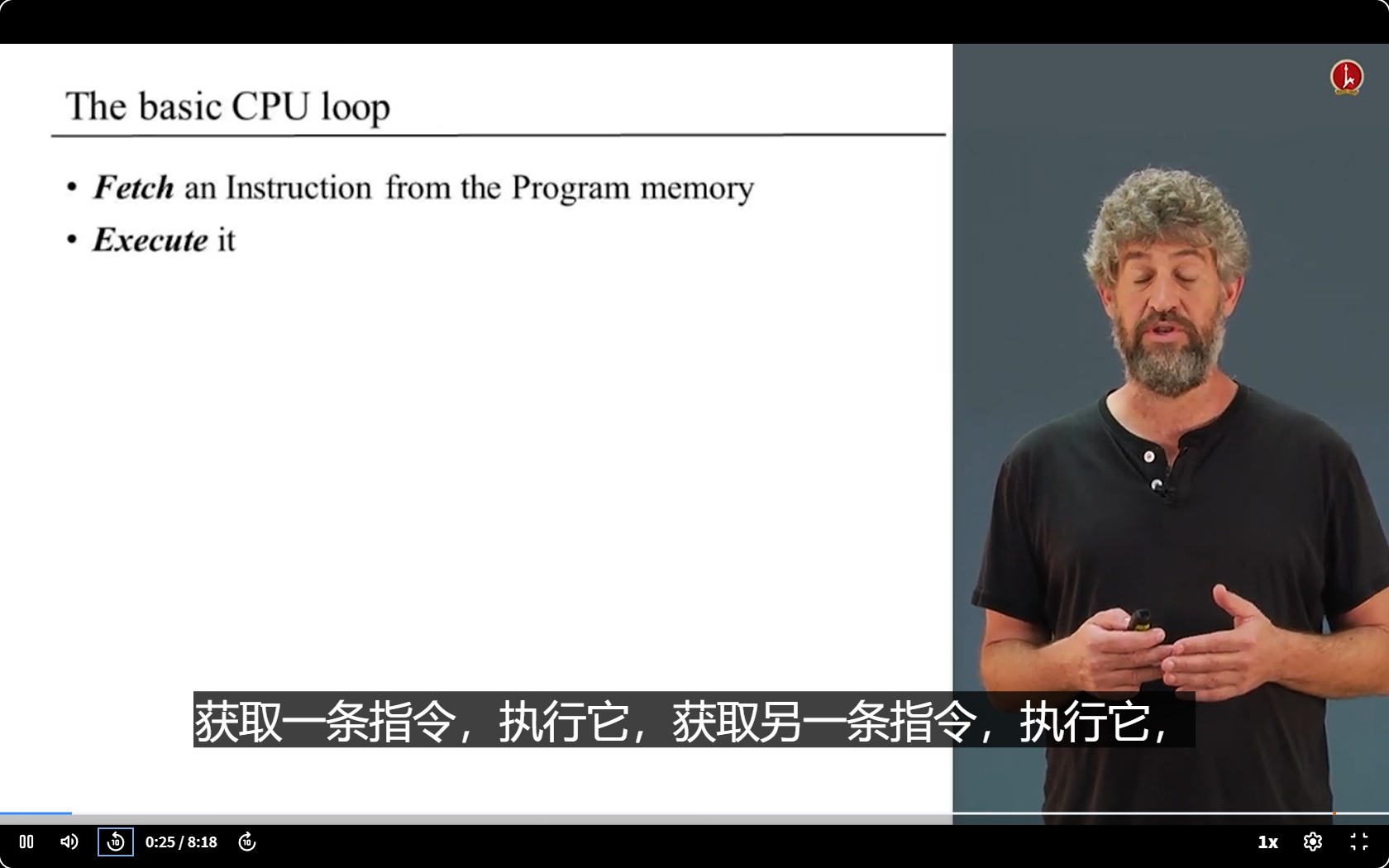
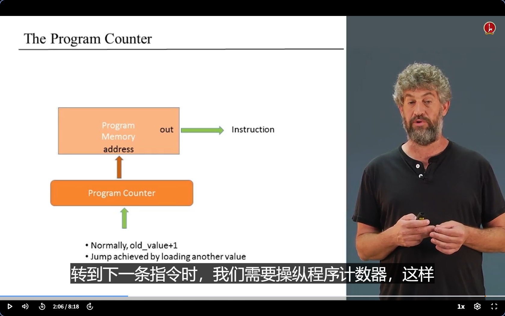
获取指令
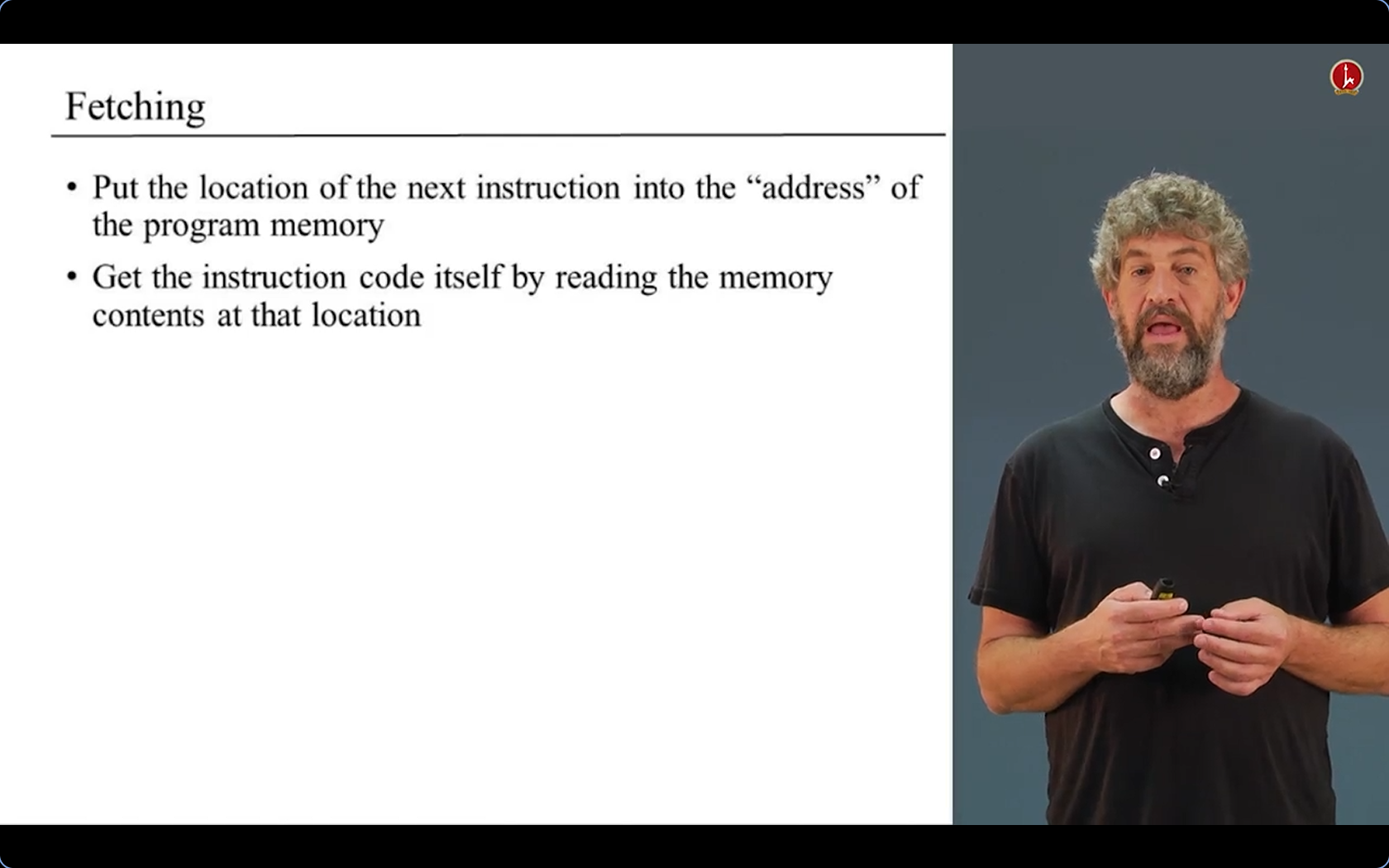
but下一条指令在哪里找呢?
在内存里
在程序内存里
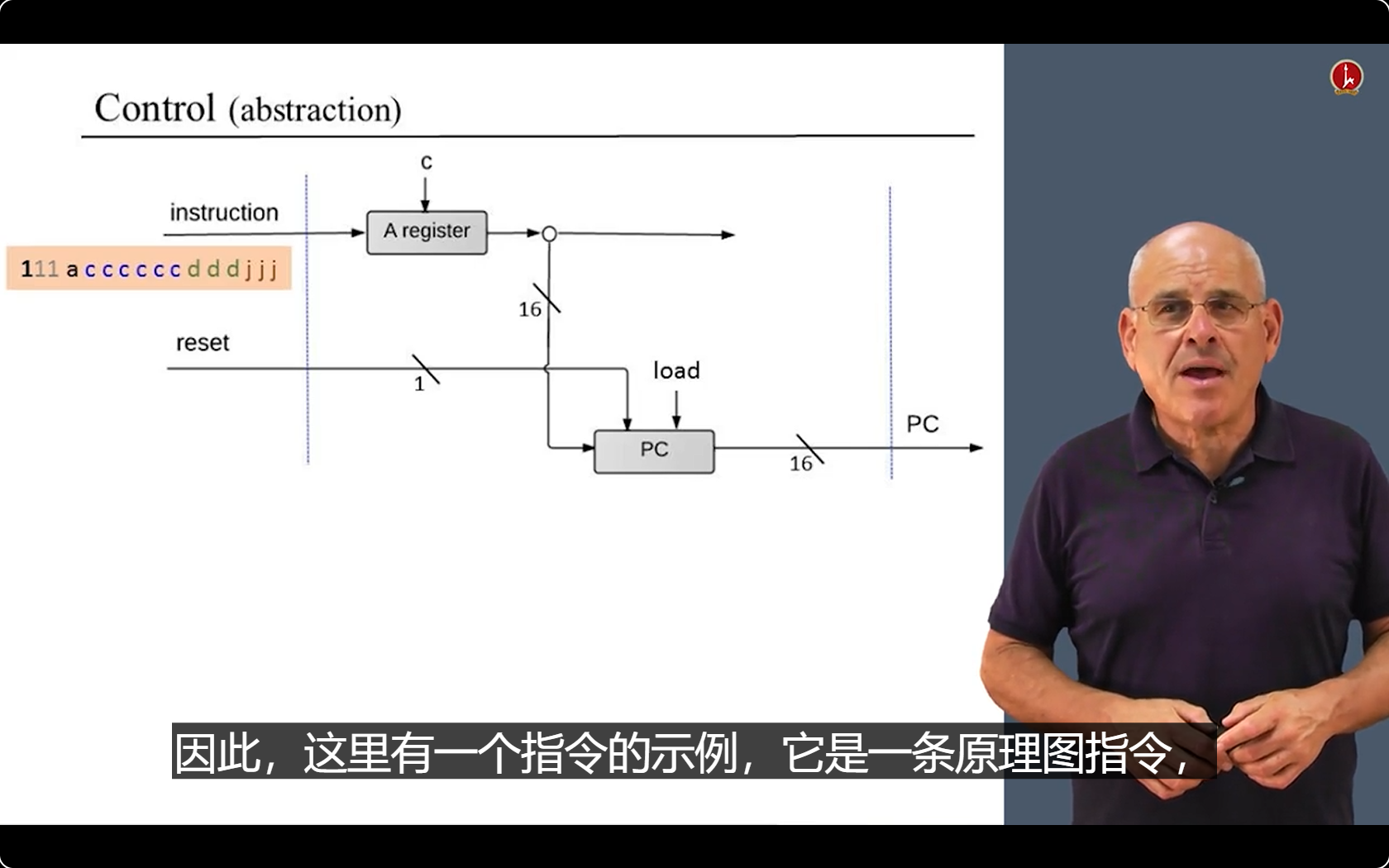
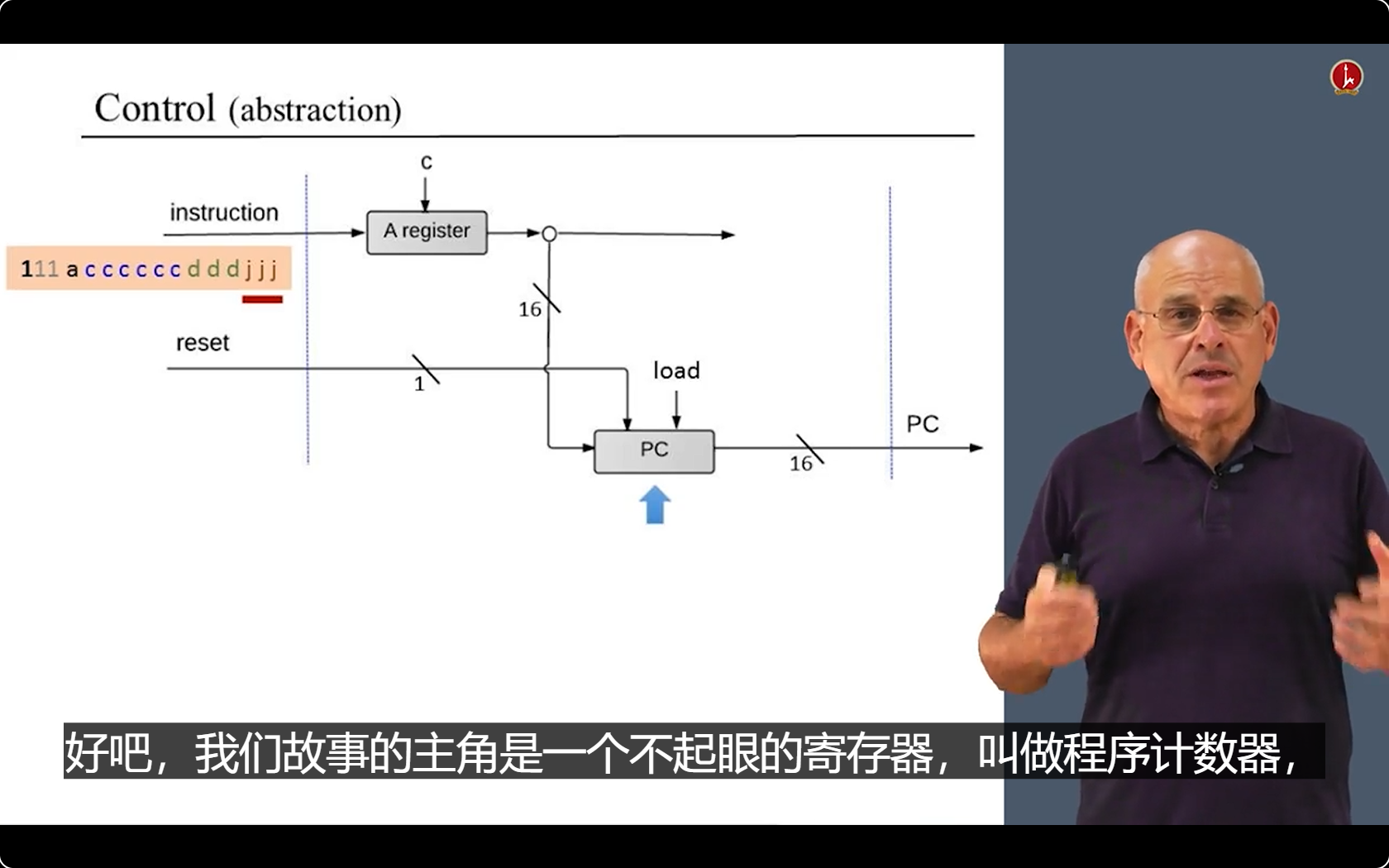
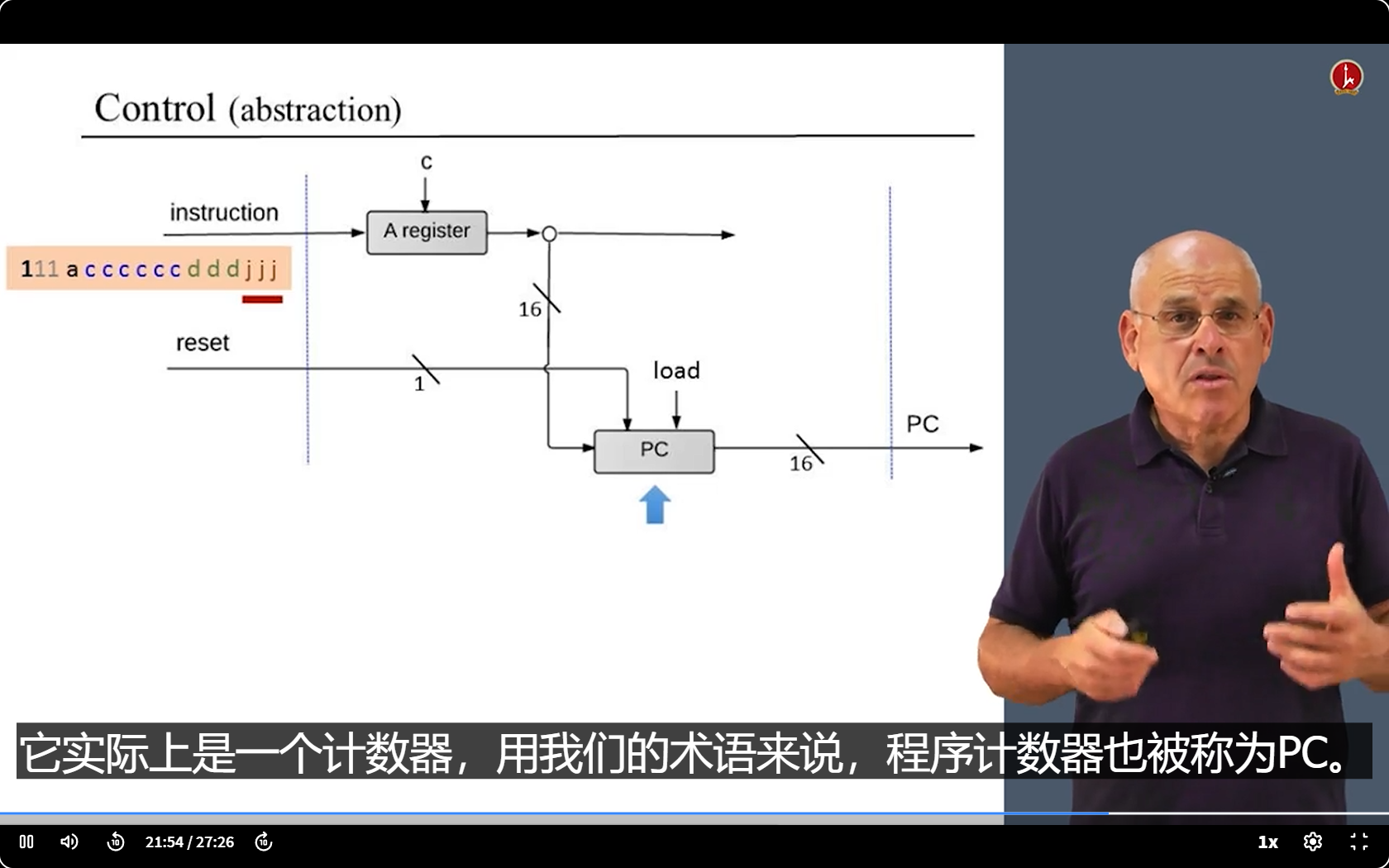
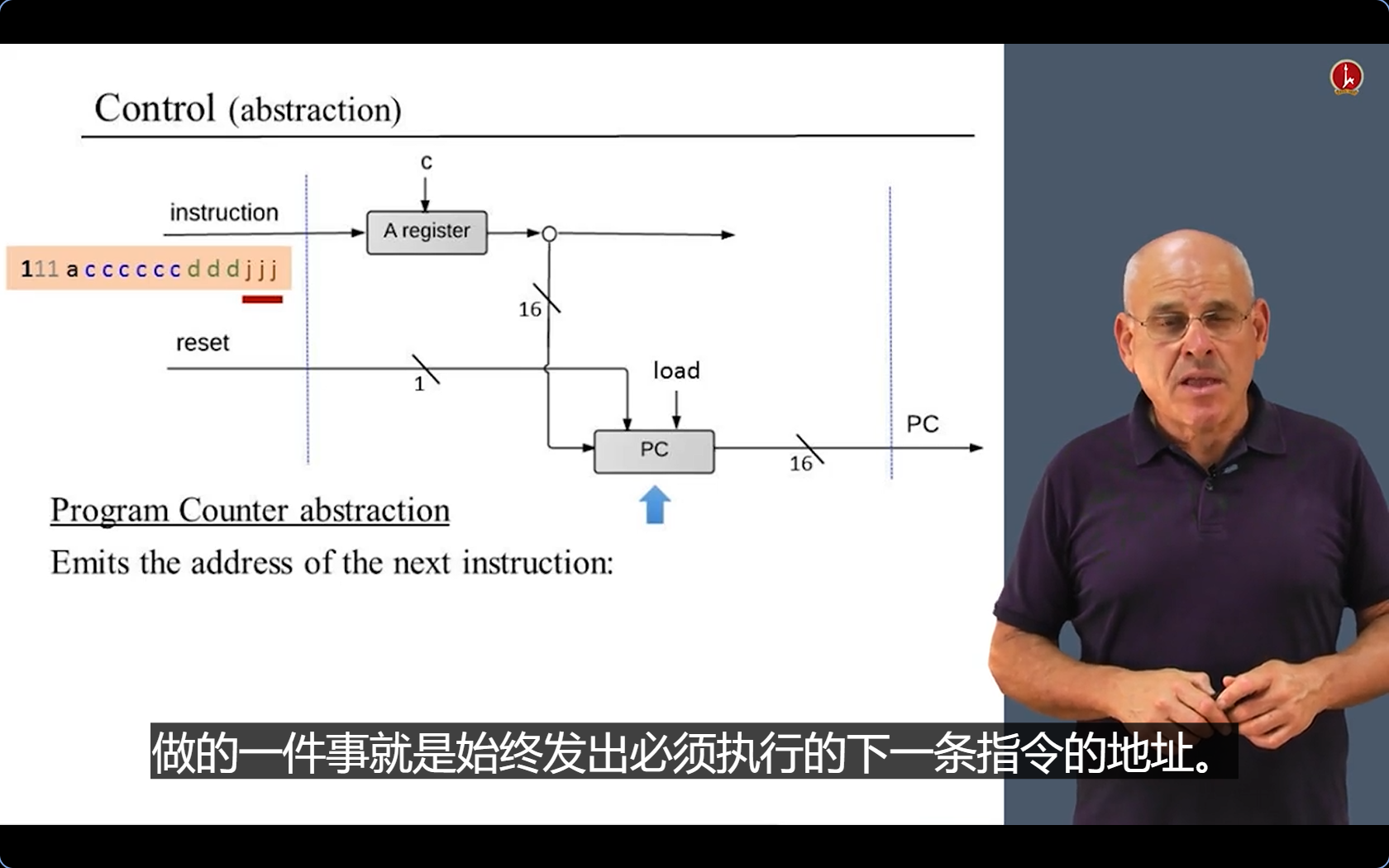
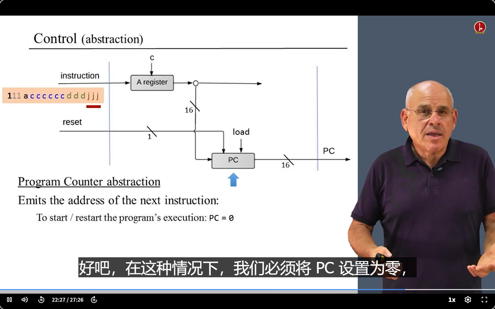
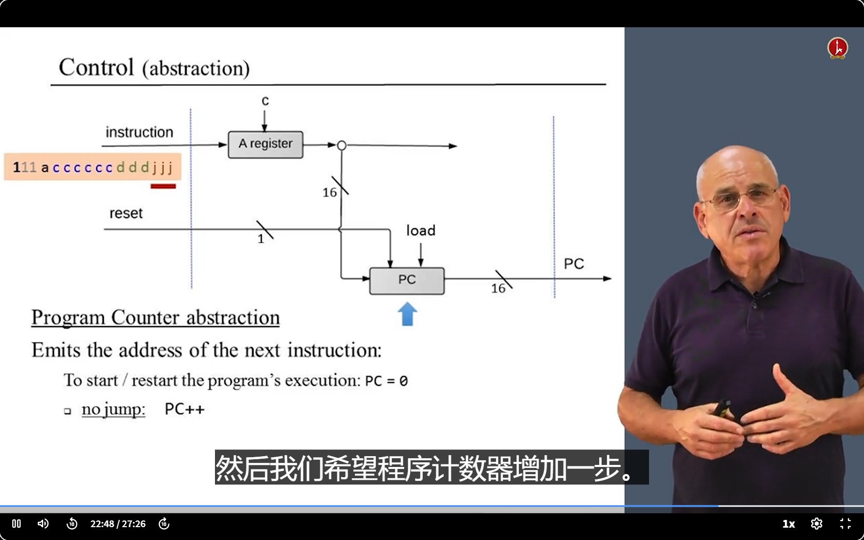
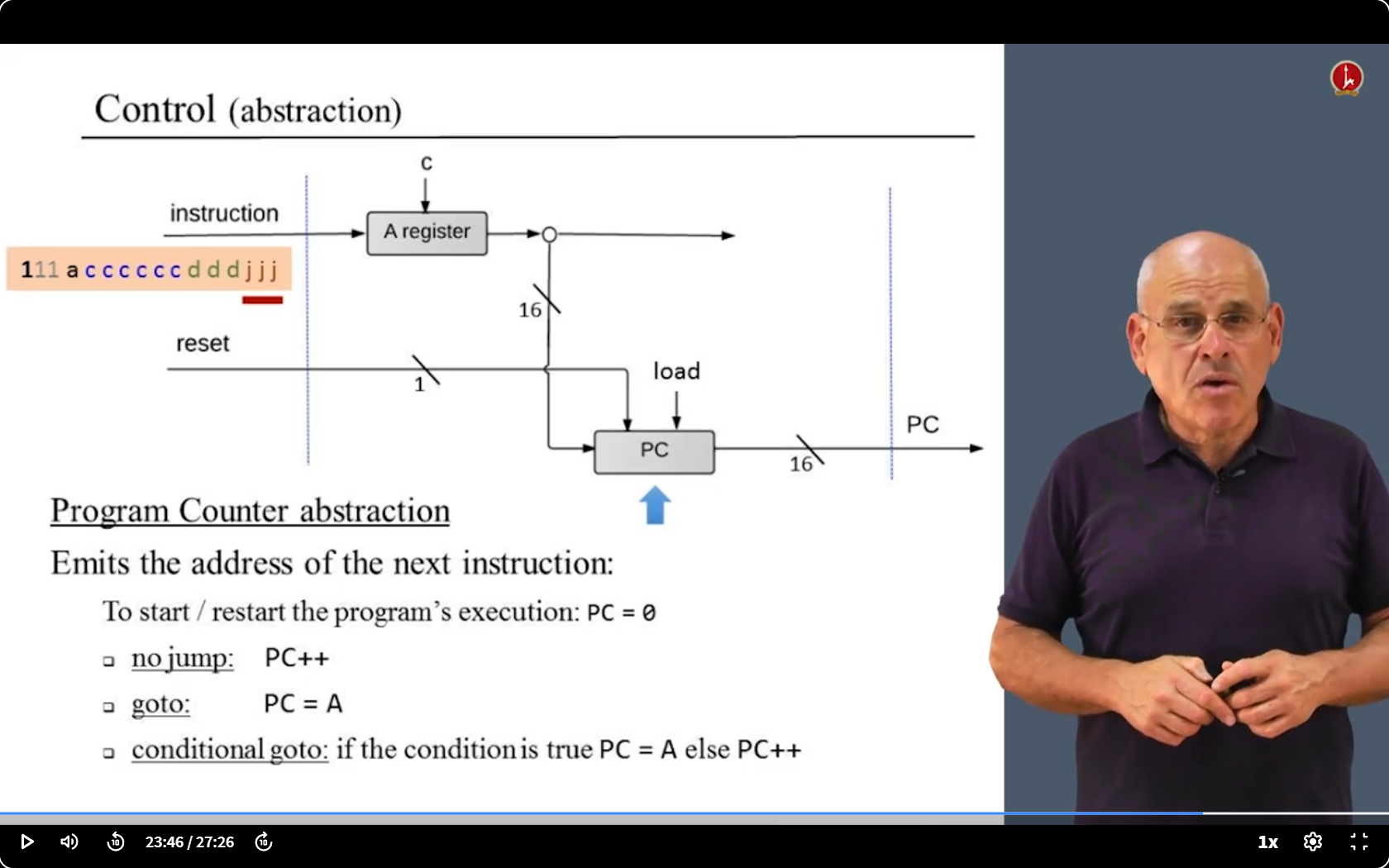
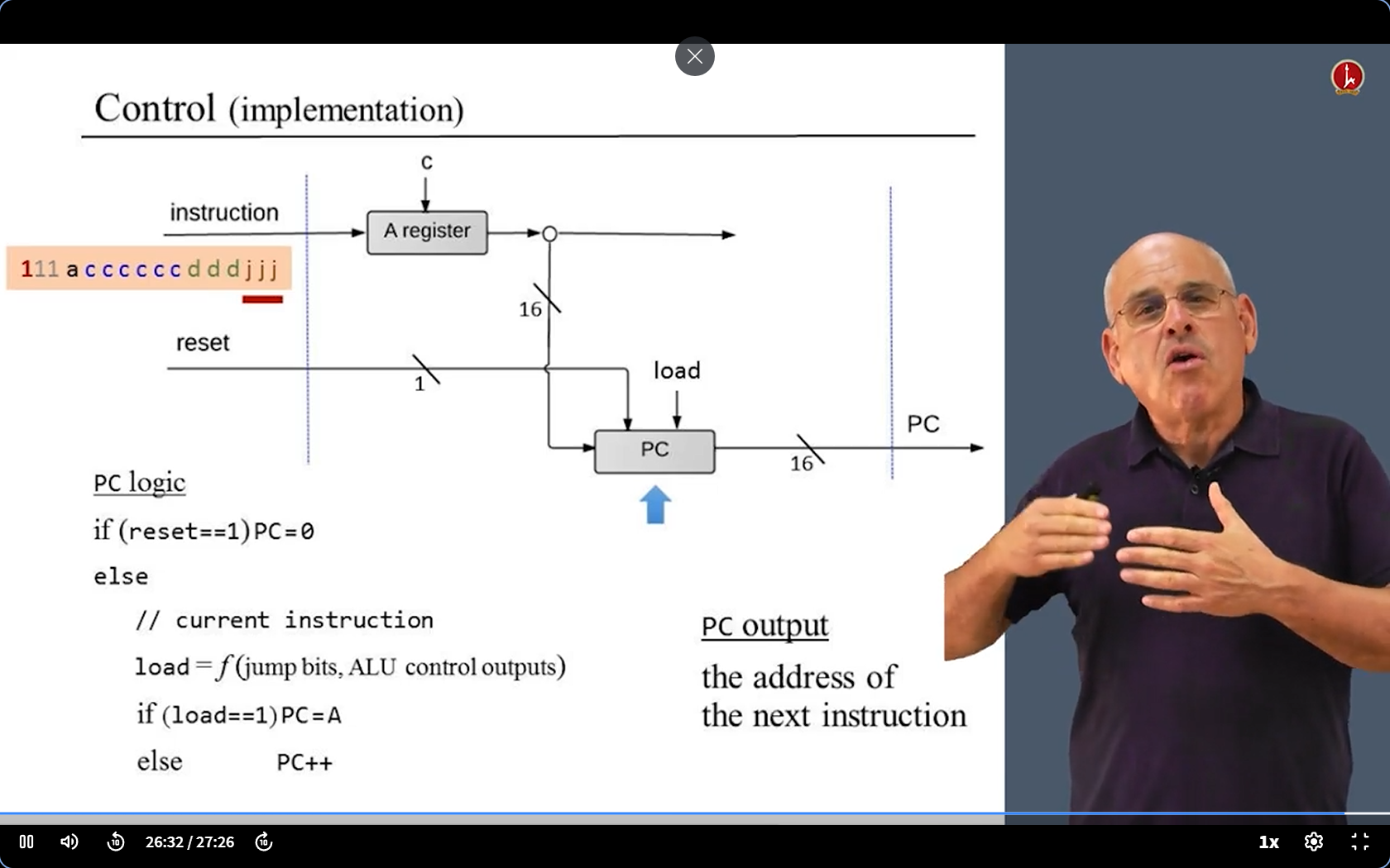
在程序计数器(program counter)里面(某个寄存器)
- 它会根据指令的执行情况自动递增或根据跳转指令等进行修改,以指向下一条要取的指令地址。
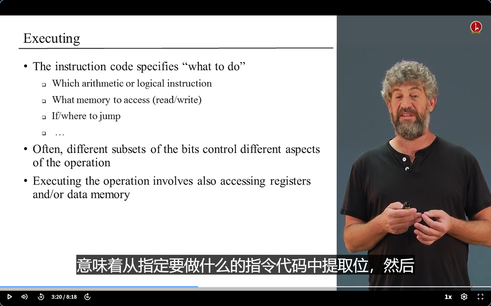
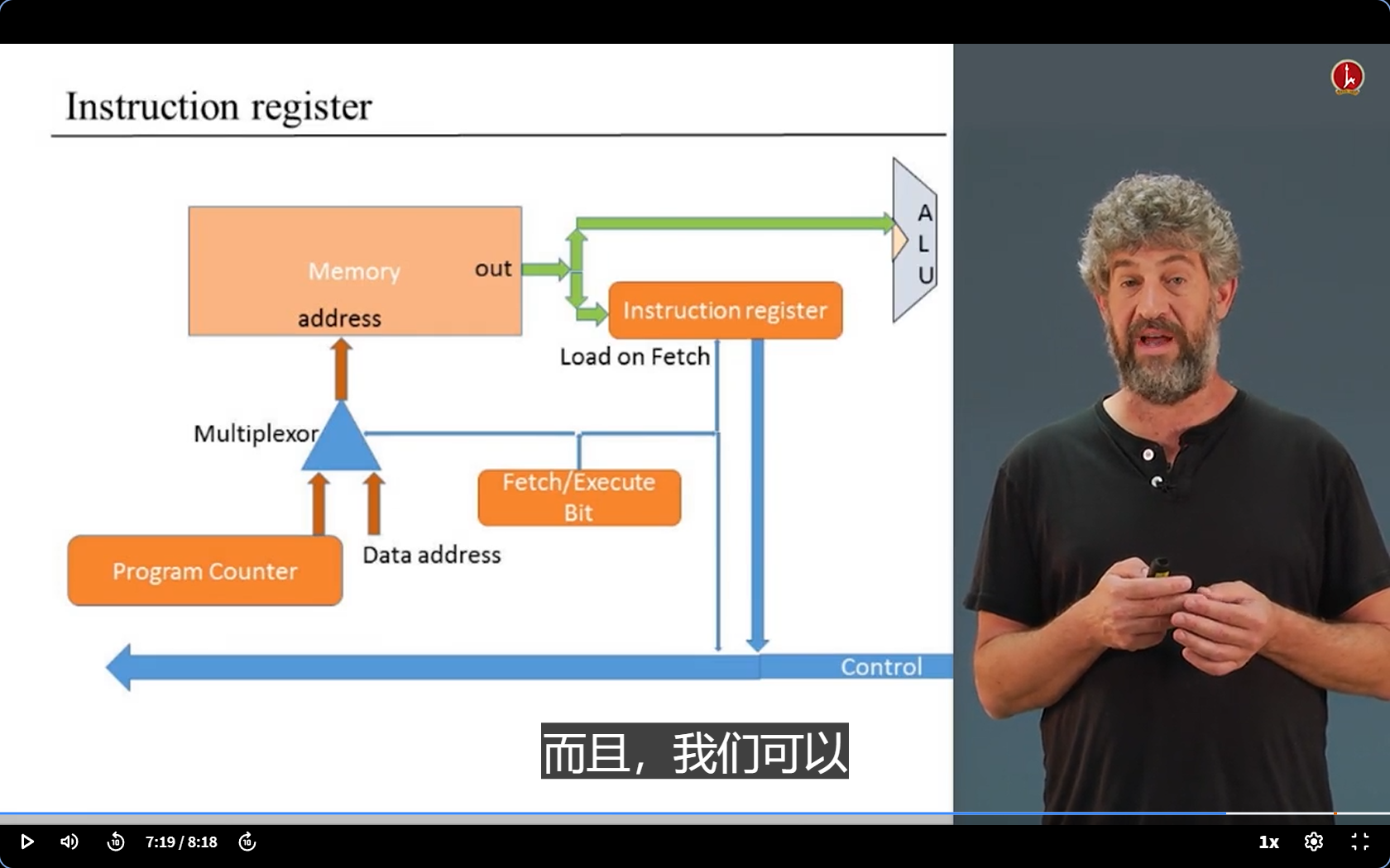
执行指令
有了Instruction,我们需要执行它。
指令代码包含了很多信息(不同位有不同信息)
把取出的指令通过 控制总线 输出到CPU
- 控制总线 告诉ALU计算什么指令,告诉数据来自哪个寄存器还是哪个数据存储器。
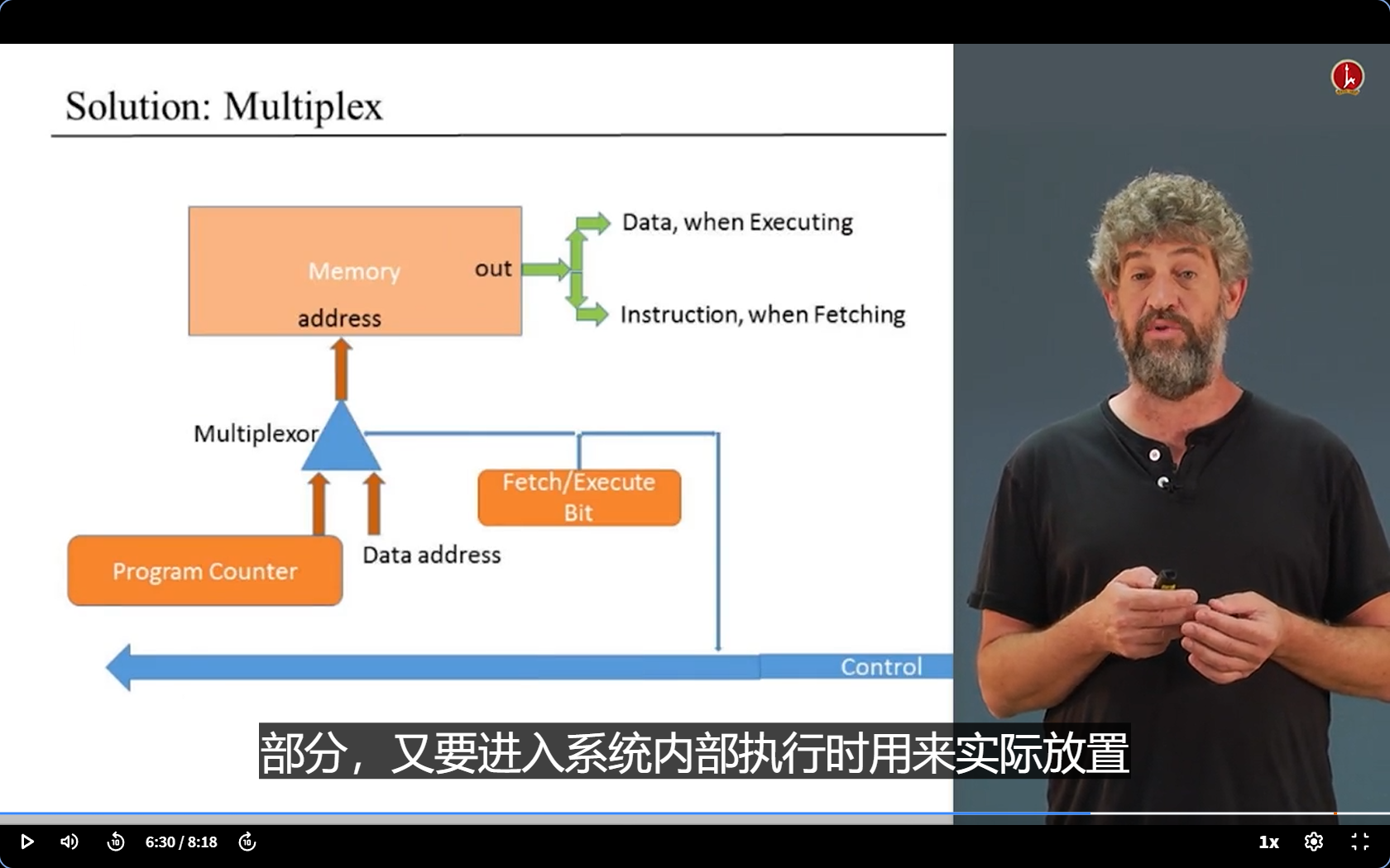
获取-执行 冲突Clash
- 简单来说,就是因为内存地址输入在同一时刻的唯一性,而取指令和执行指令时都需要使用内存地址来获取不同的内容(指令和数据),从而导致了冲突。
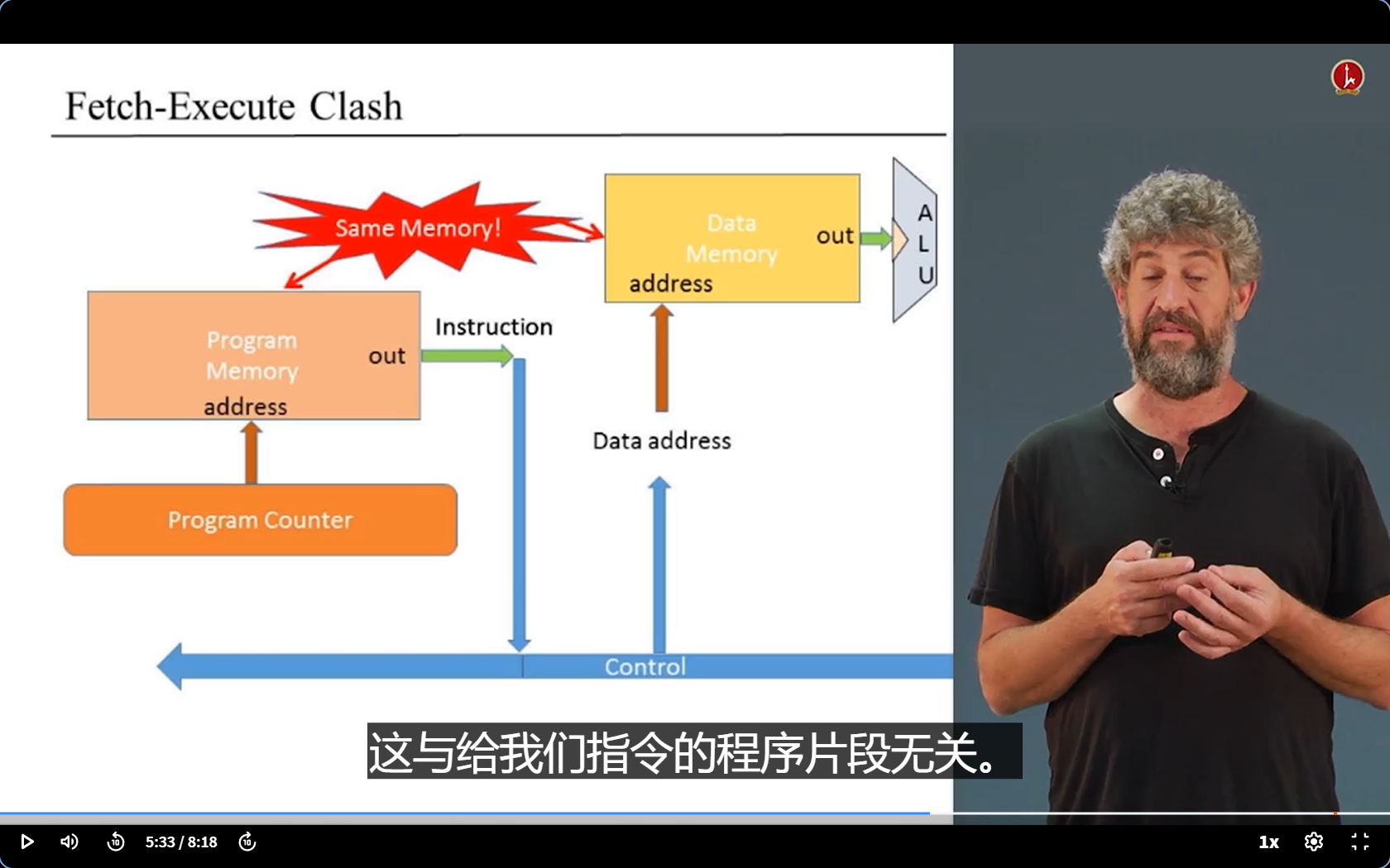
- 解决方法:一个一个做。通过一个Mux解决(sel:a Fetch/Execute Bit)
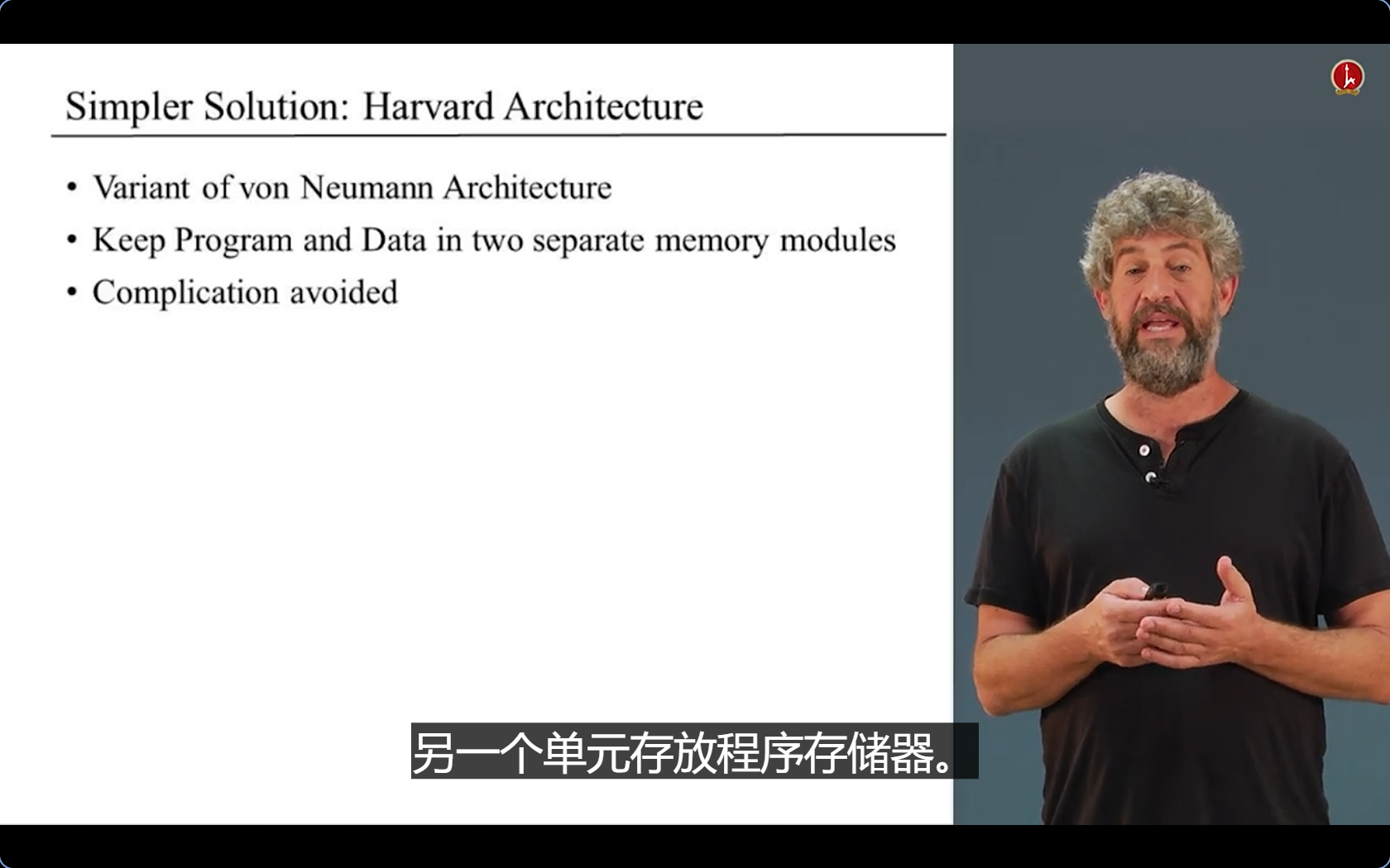
- 更简单的解决方法:把内存分为两个部分,一个部分作为数据存储器,另一个办法作为程序存储器。
Next
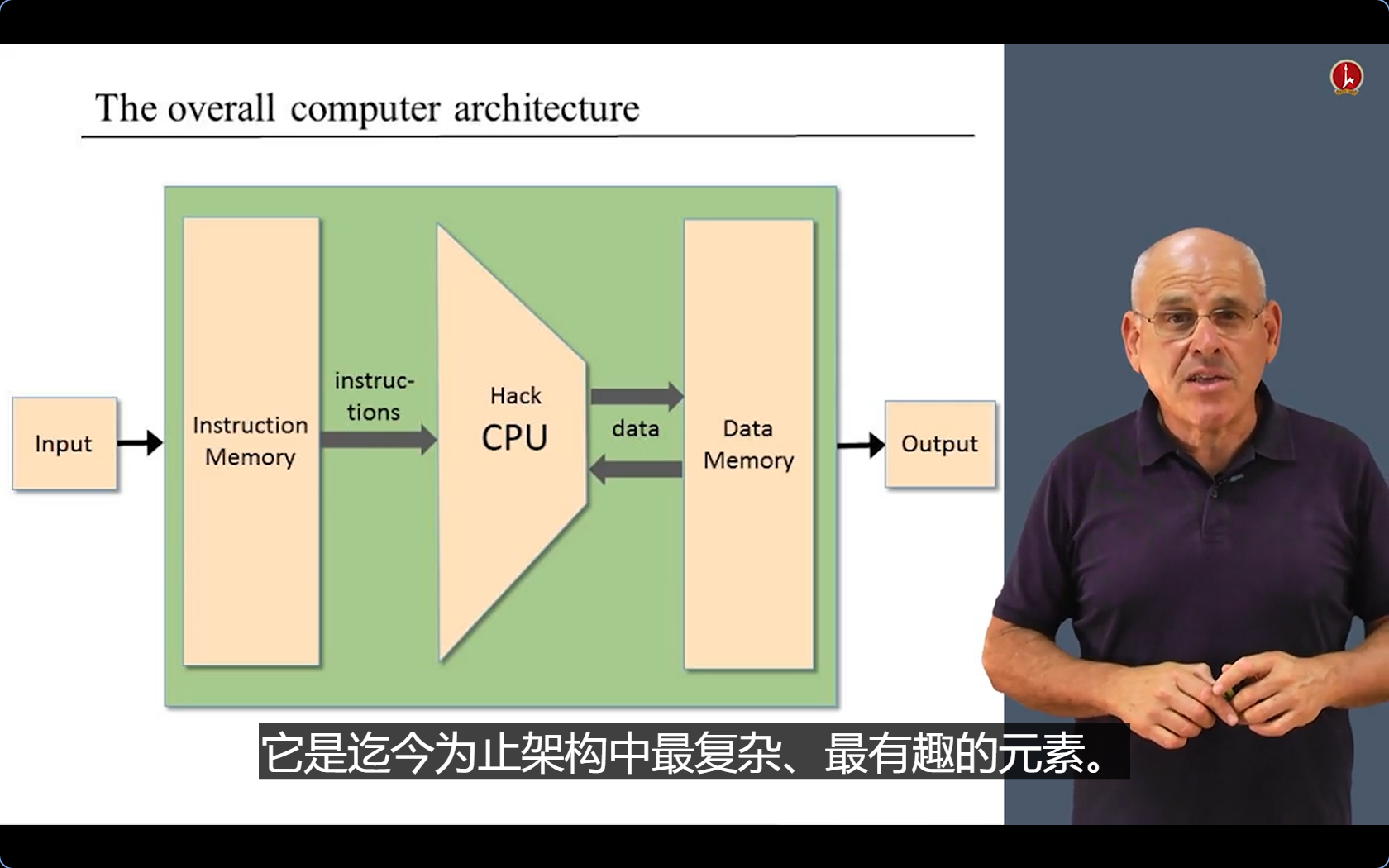
- 这一节,我们讨论了计算机的一般架构
- 下一节,我们讨论我们的HACK计算机
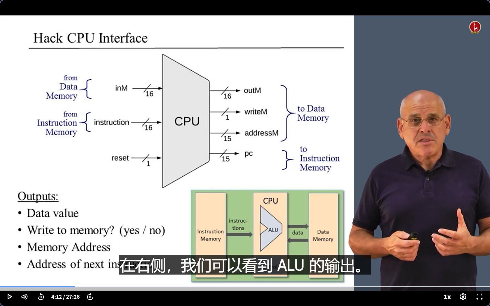
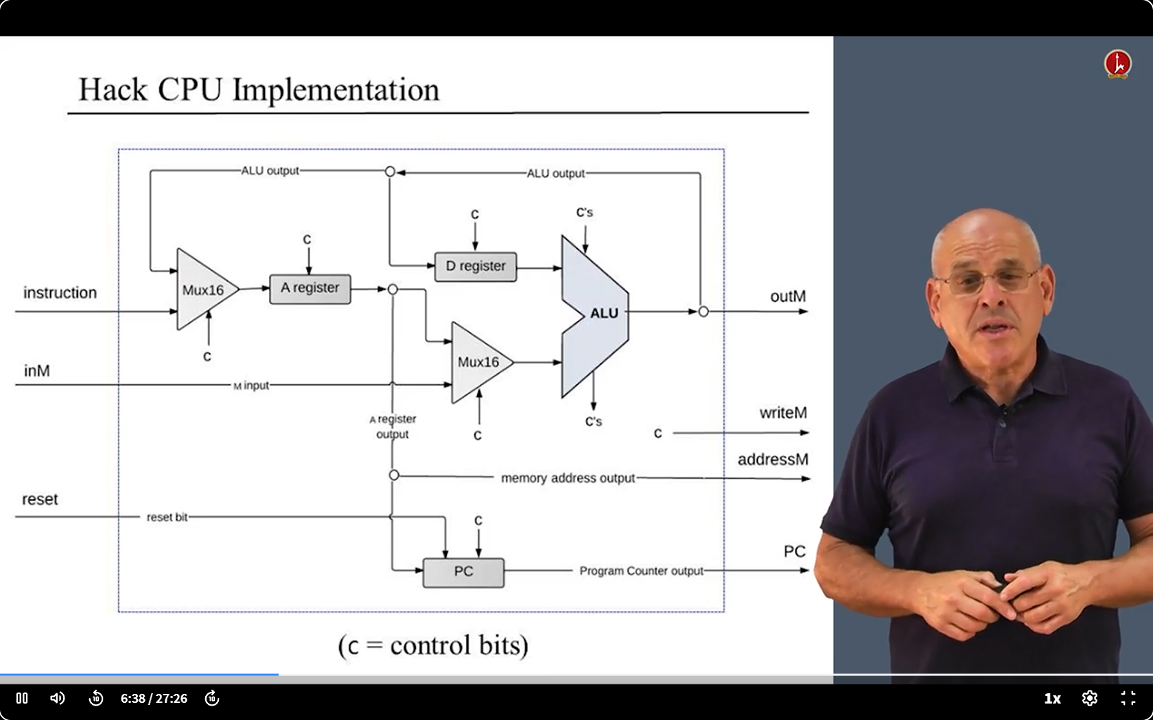
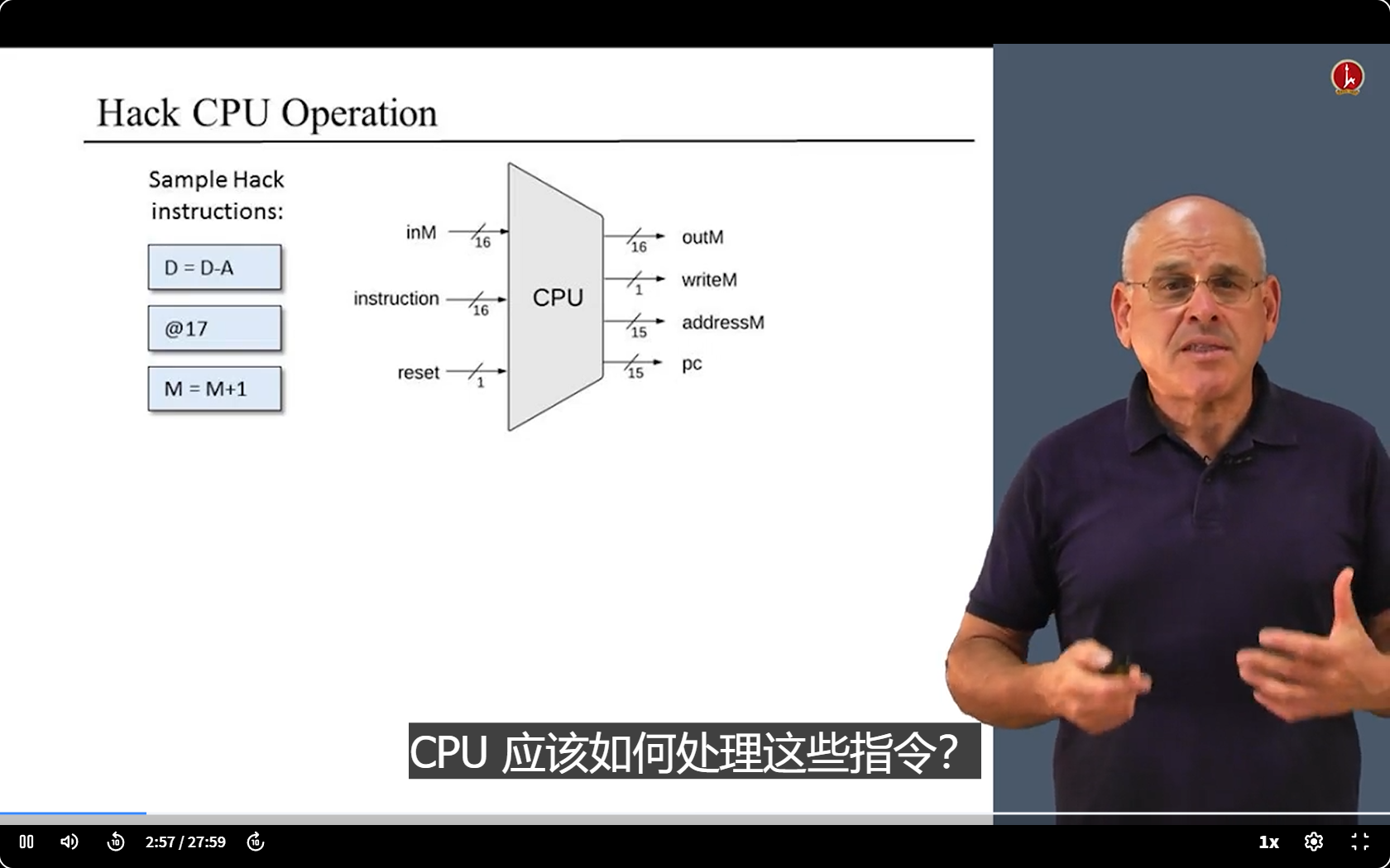
5.3 Central Processing Unit
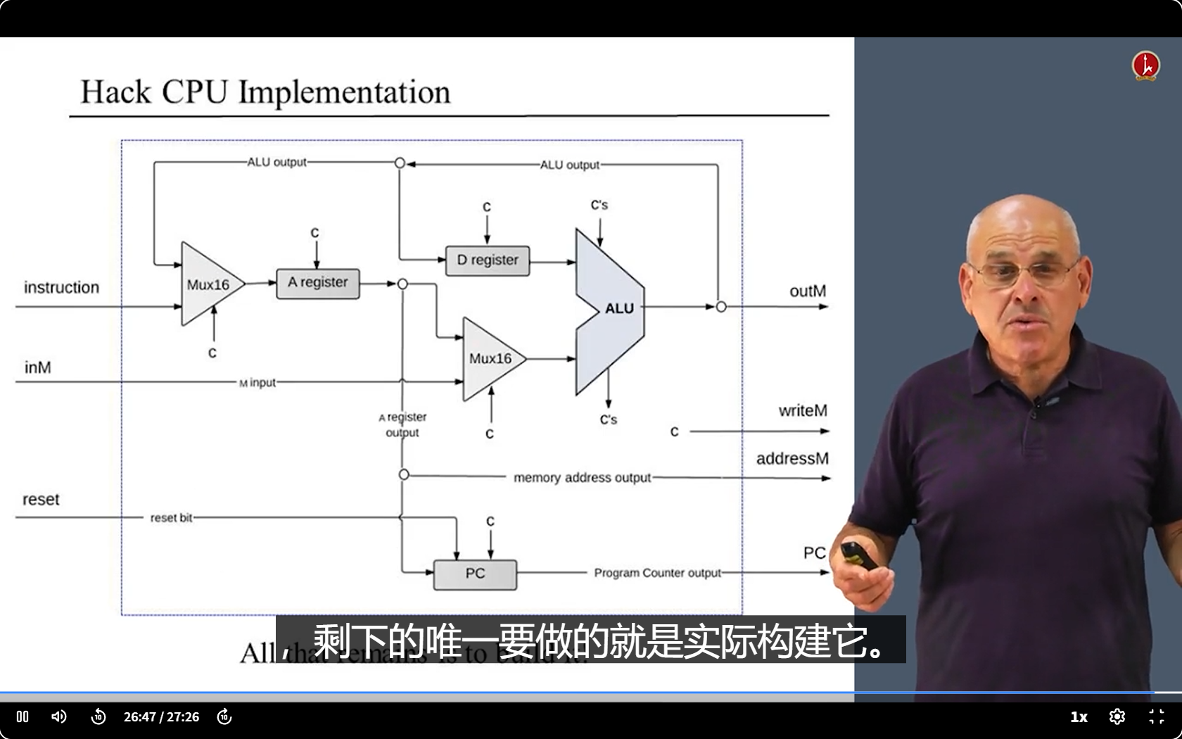
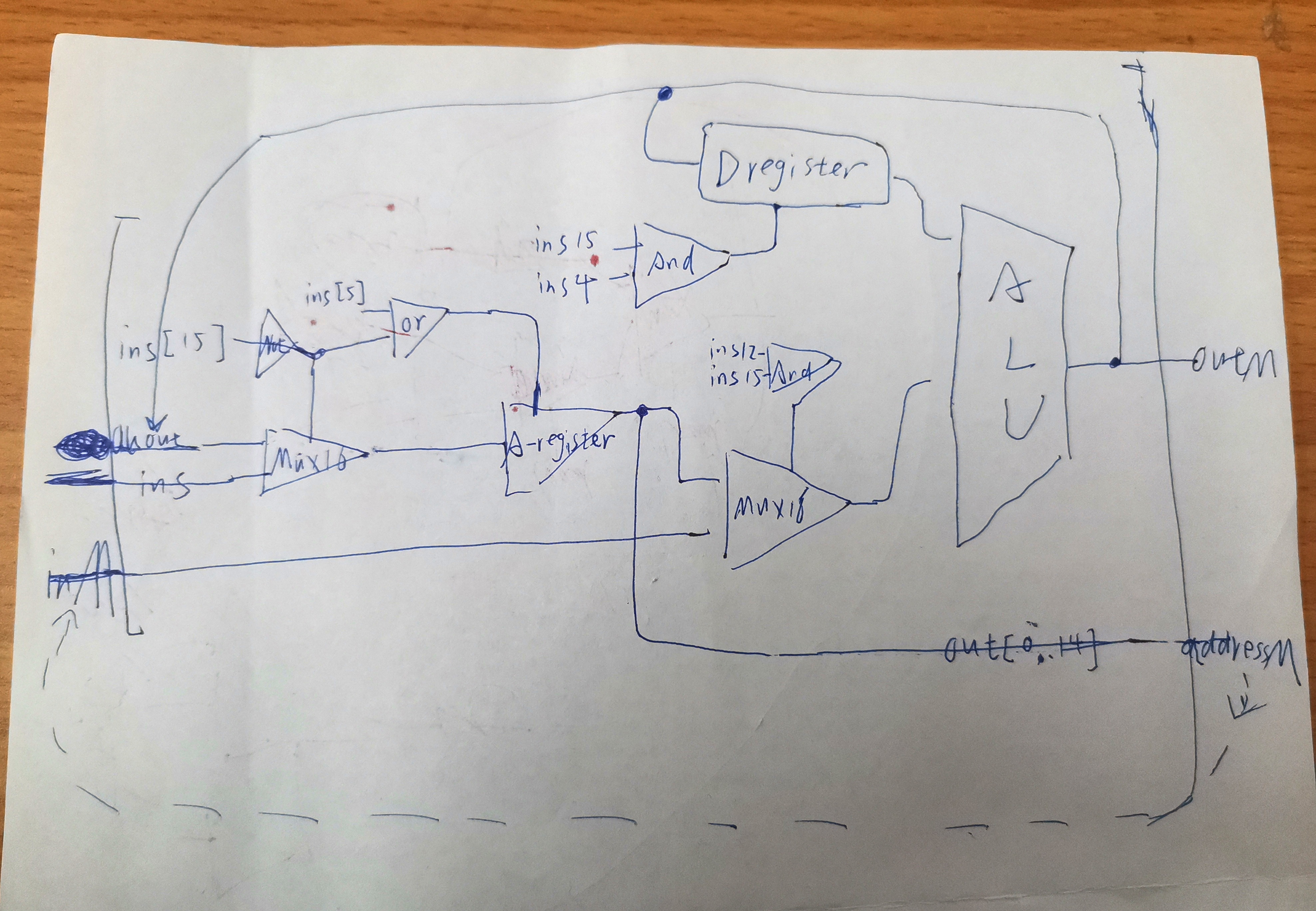
CPU: interface and implementation
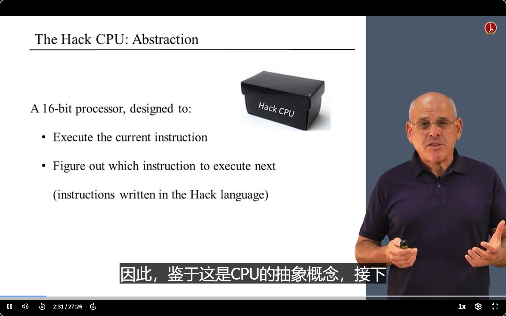
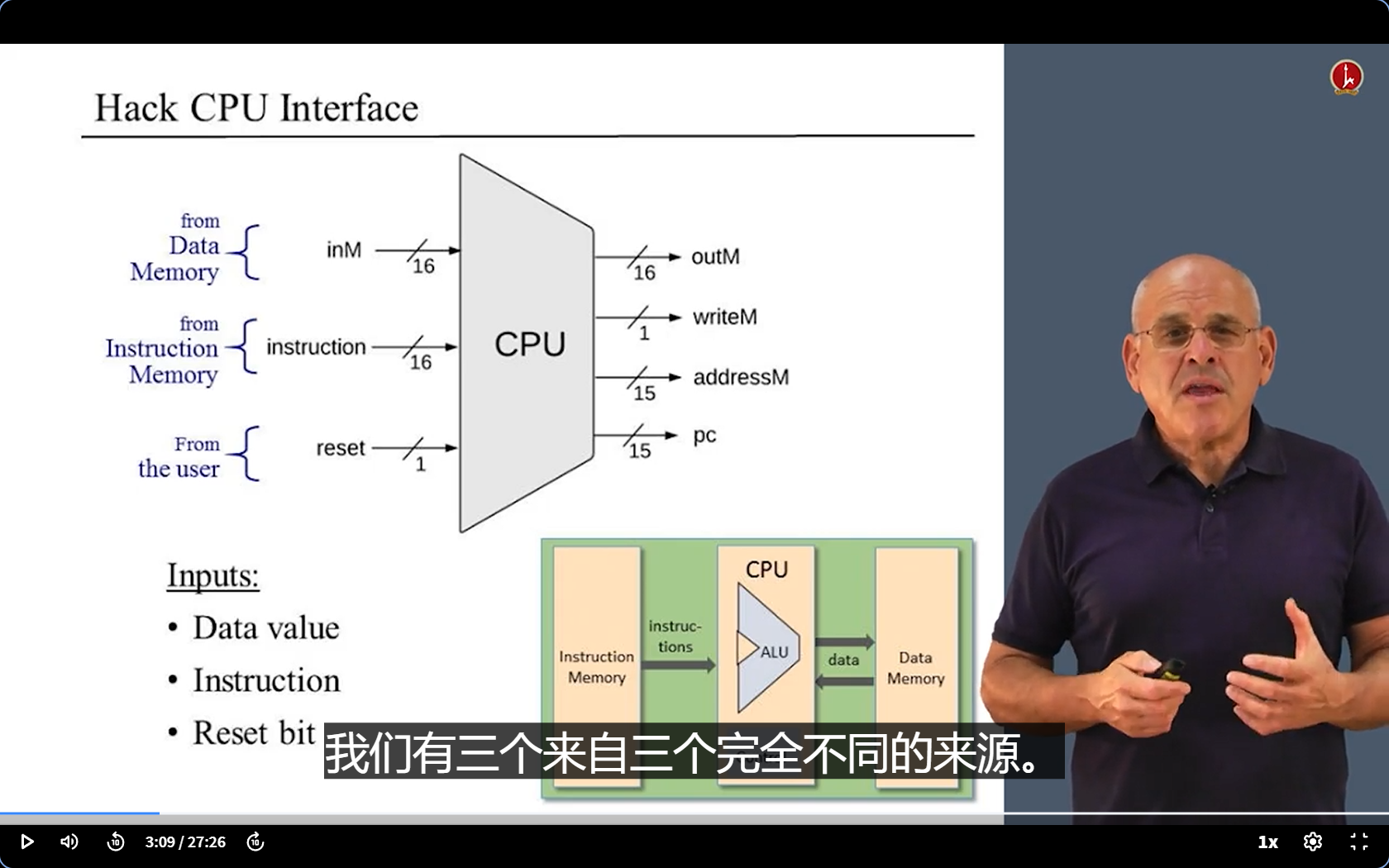
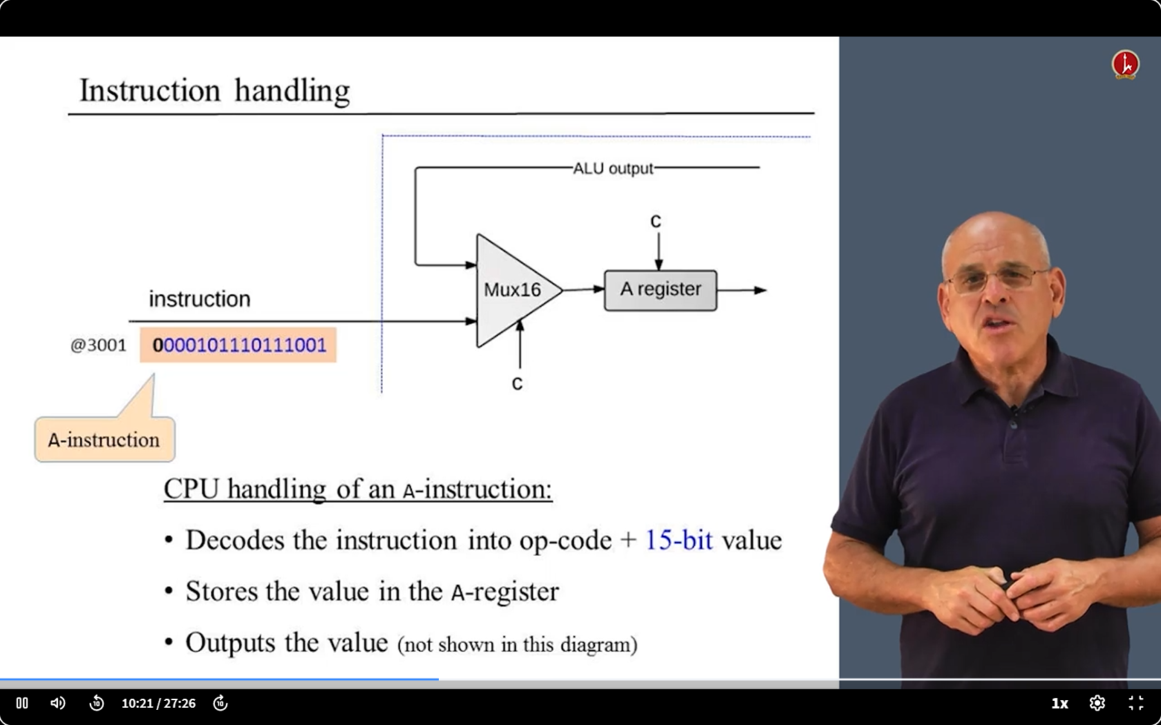
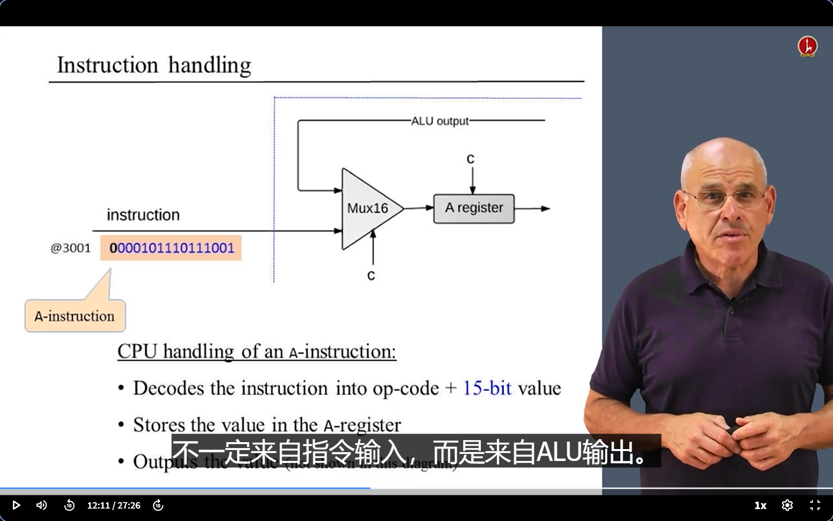
CPU: Instruction handling
handle A-instruction
地址寄存器
解码:分离操作码(最前面一位,就是instruction[15] )和其他字段(15位的地址或是值)
确定是A指令后,取出后15位值,把它放入A寄存器中。
CPU 同时做的另一件事:取出A寄存器的输出(后15位,ins[0..14] ),并通过我们称之为“M地址”的输出将其输出到CPU外部。
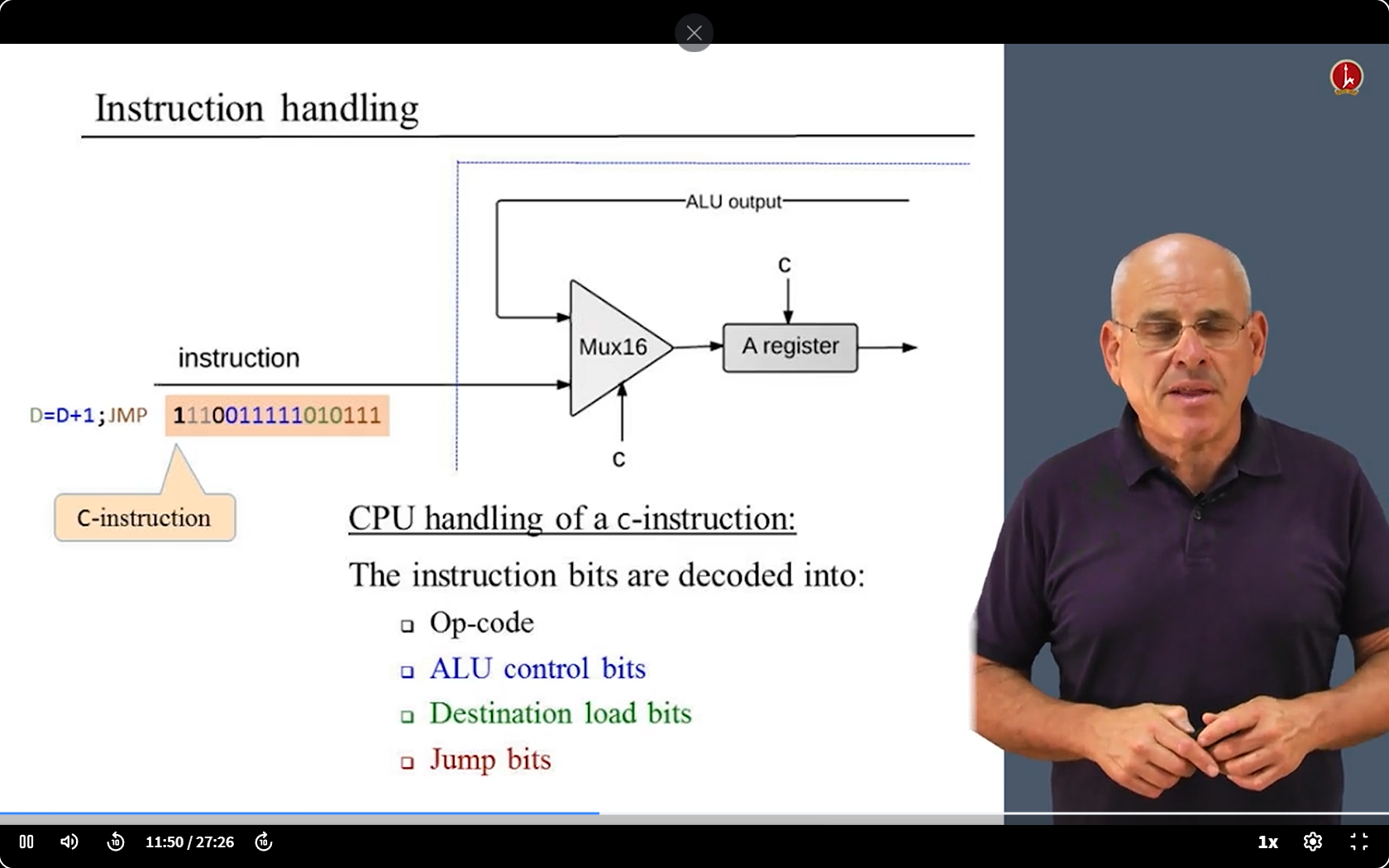
handle C-instruction
- 解码:分离操作码和其他三个字段
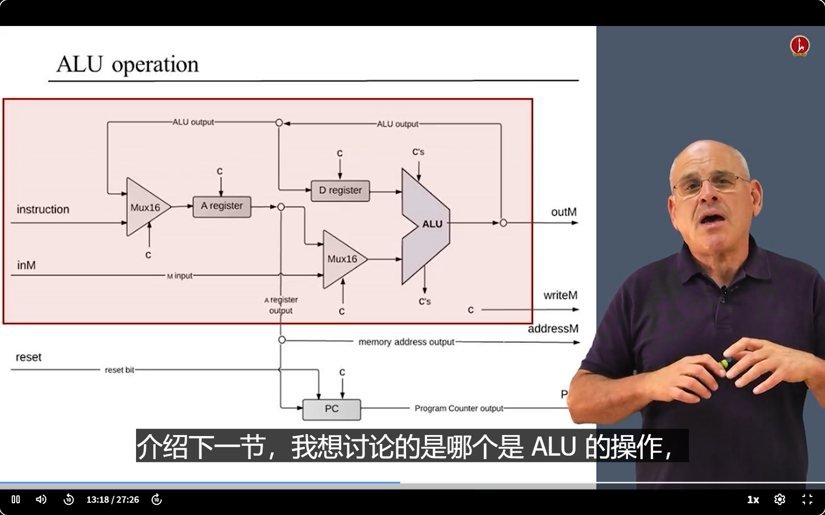
A regester – again
- 我们发现:A寄存器也可以由 ALU的输出 提供数据,而不一定是来自指令输入。(是不是有时候ALU发现该跳转了,所以输出指令给A regester?)
- 在某些情况下是操作码为0的A指令,在这种情况下,我们希望输入来自指令。
- 在其他情况下是操作码为1的C指令,在这种情况下,我们希望以某种方式路由A寄存器的输入,使得输入来自ALU。
- 例如,如果 C 指令是要计算某个数值与 A 寄存器当前值的和,那么 ALU 会从 D 寄存器(或其他数据源)和 A 寄存器获取操作数进行加法运算,运算结果可能需要再存回 A 寄存器,所以就需要将 ALU 的输出路由到 A 寄存器作为其输入。(就不用inM了)
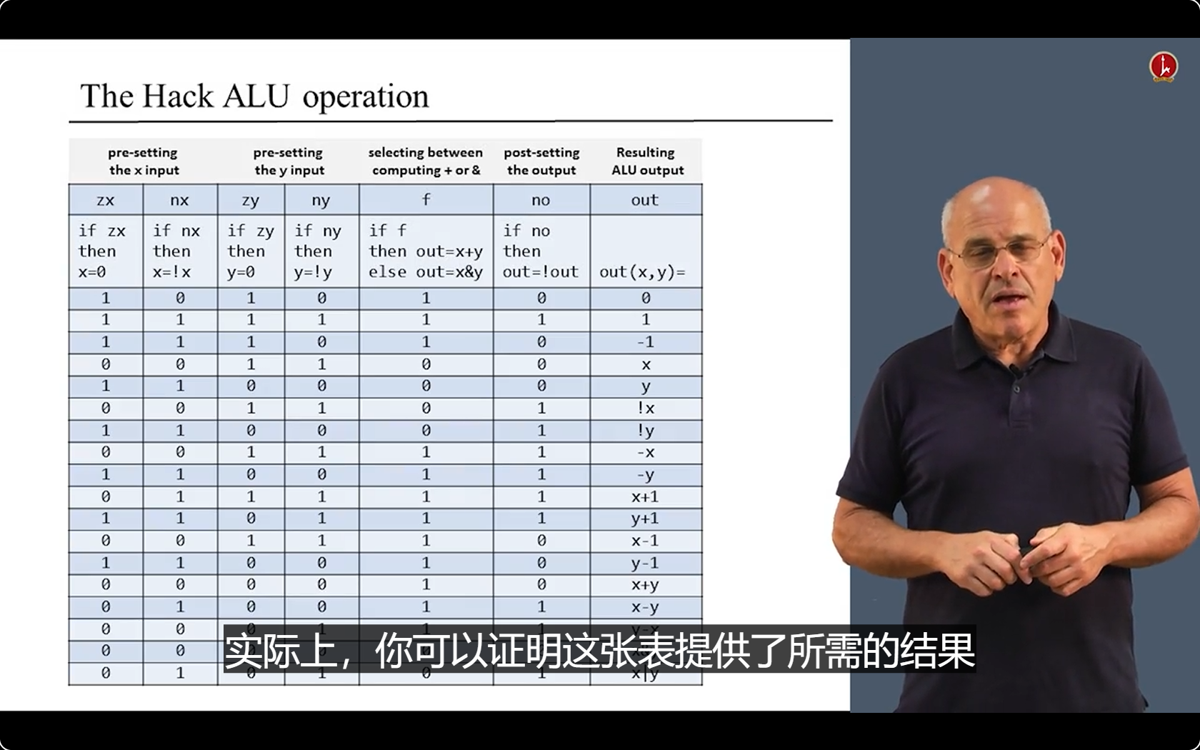
CPU: ALU operation
ALU operation: inputs
- remember:C指令由不同的位字段组成,每个字段都有不同的含义。
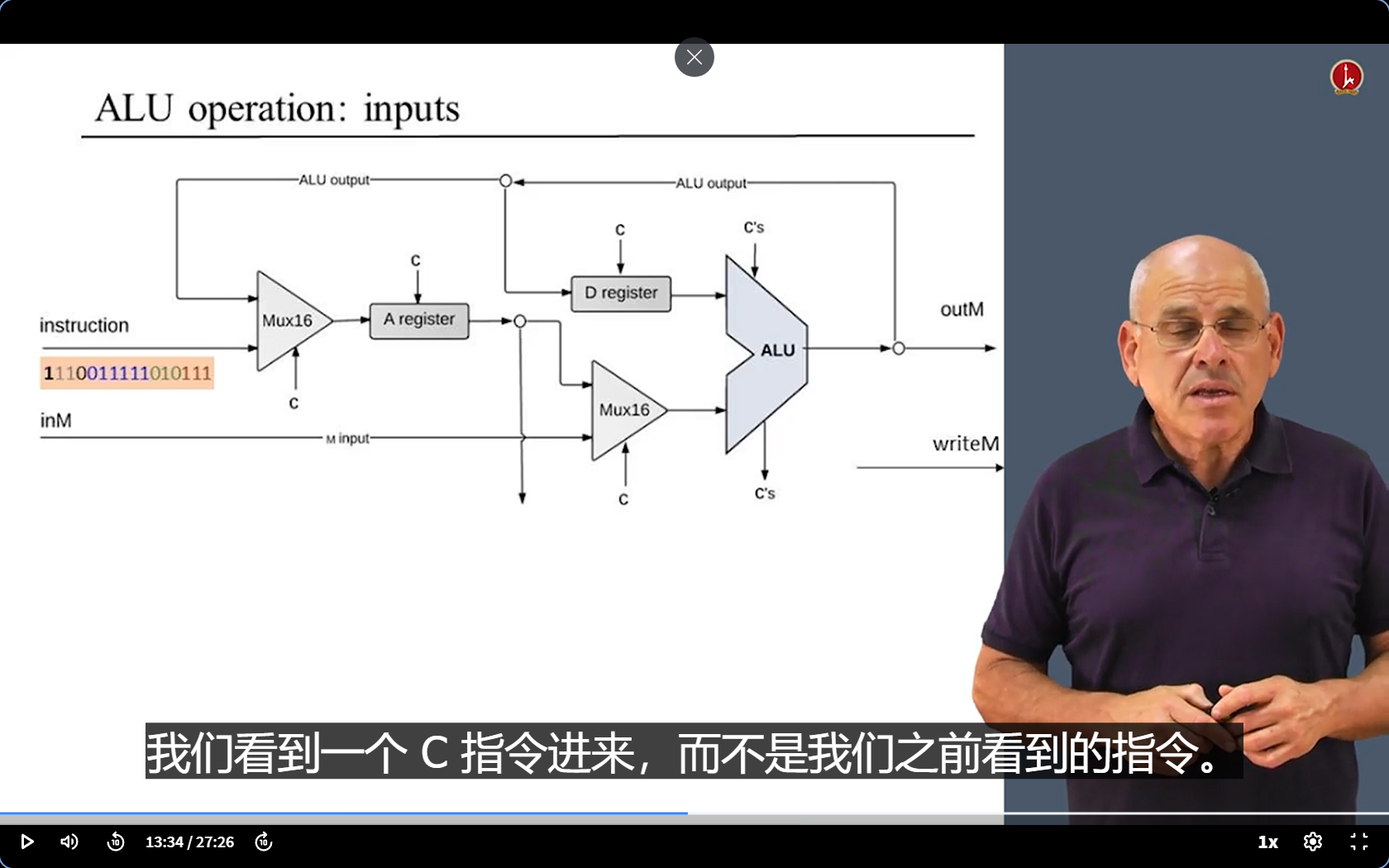
- ALU 有两个输入源 , 最终输入depend on 控制位c和011111(now)
- Control bit from the instruction
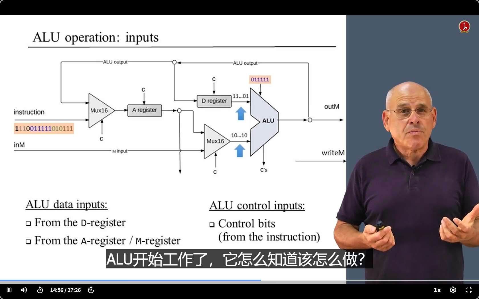
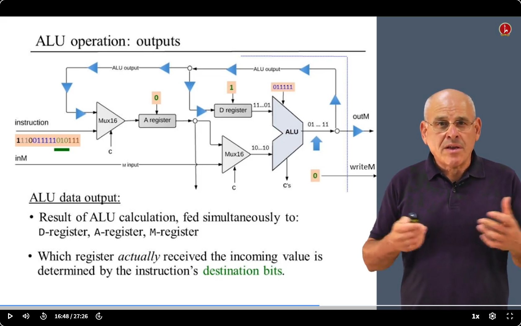
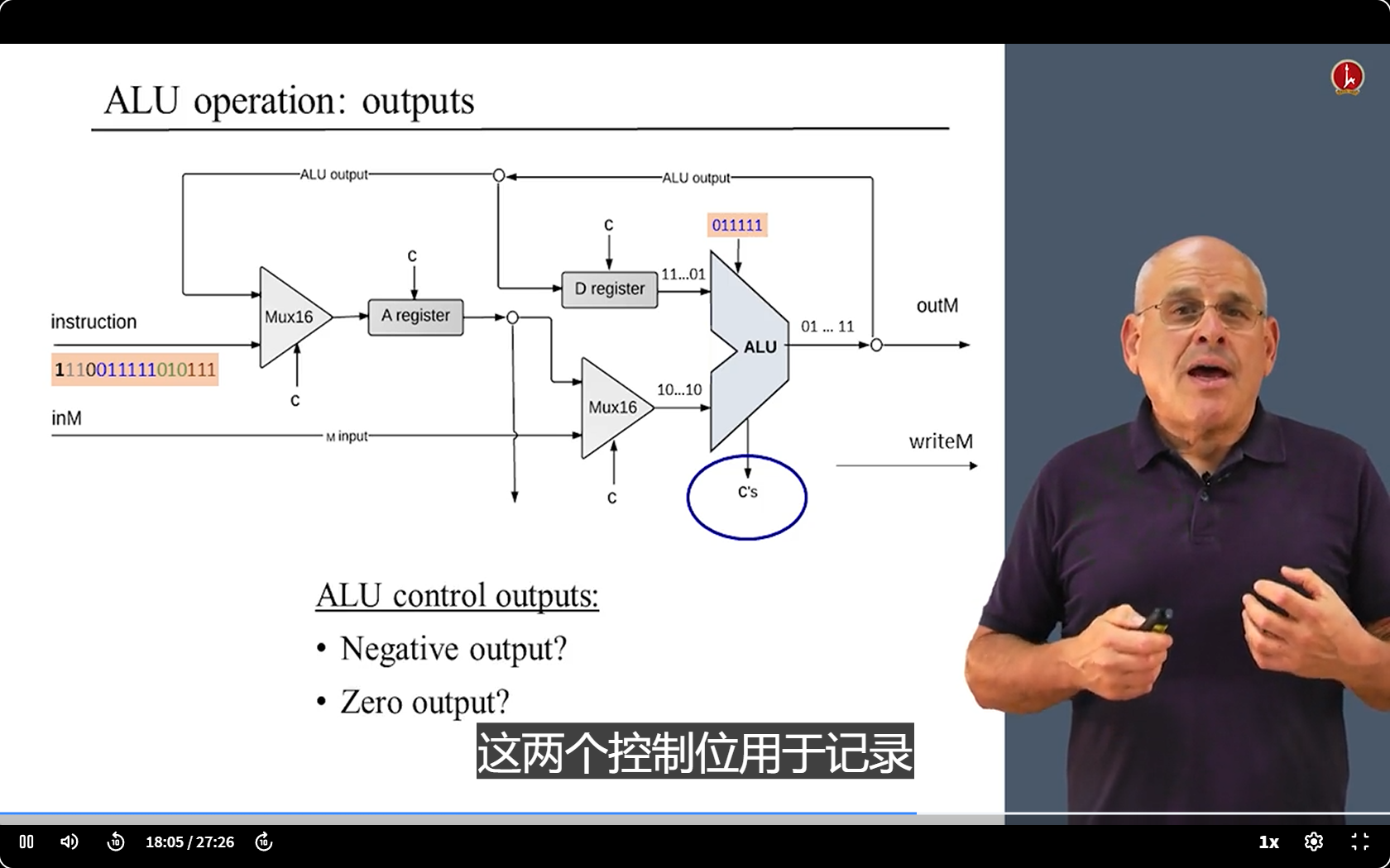
ALU operation: outputs
- ALU 的 输出被送到三个地方。
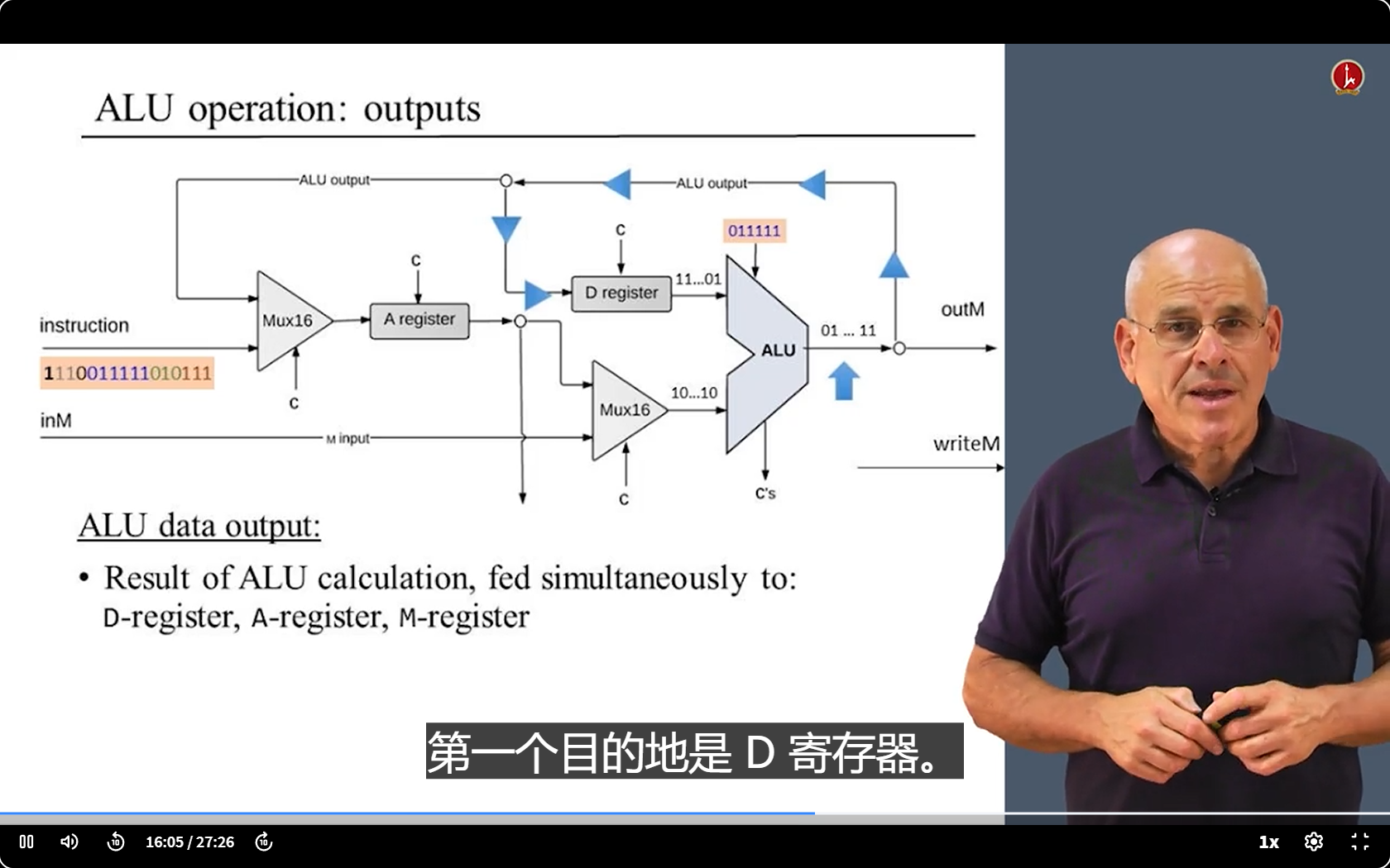
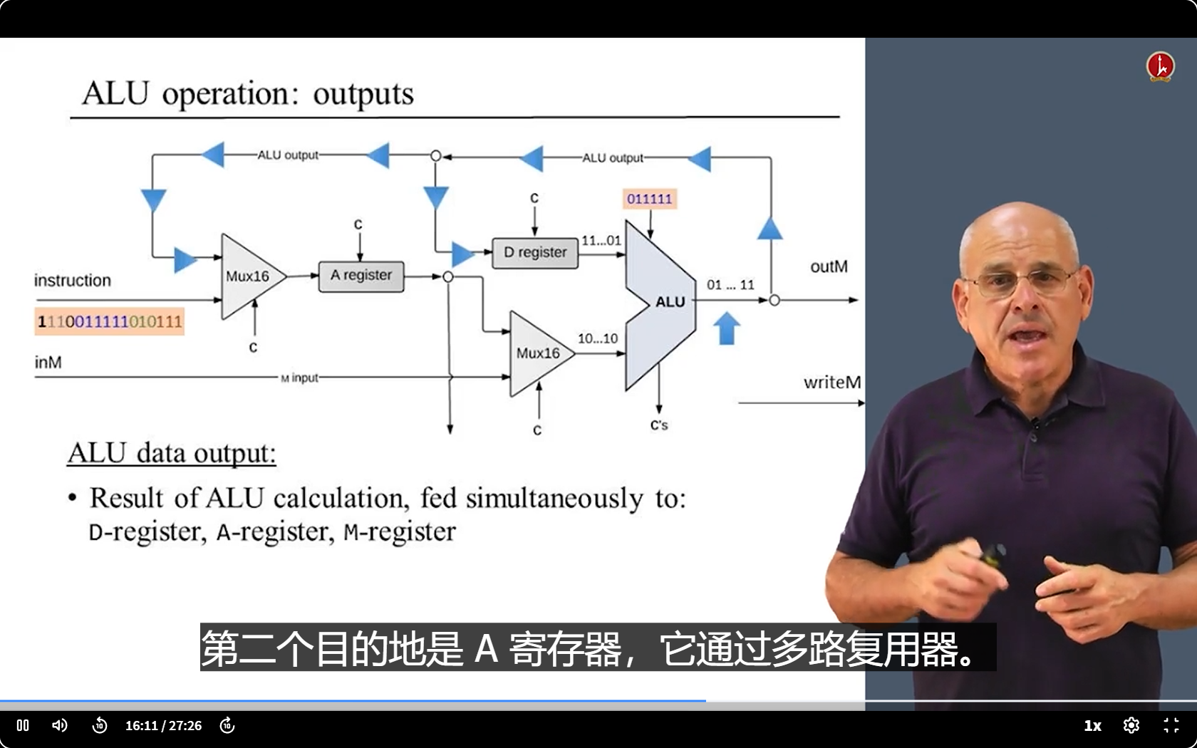
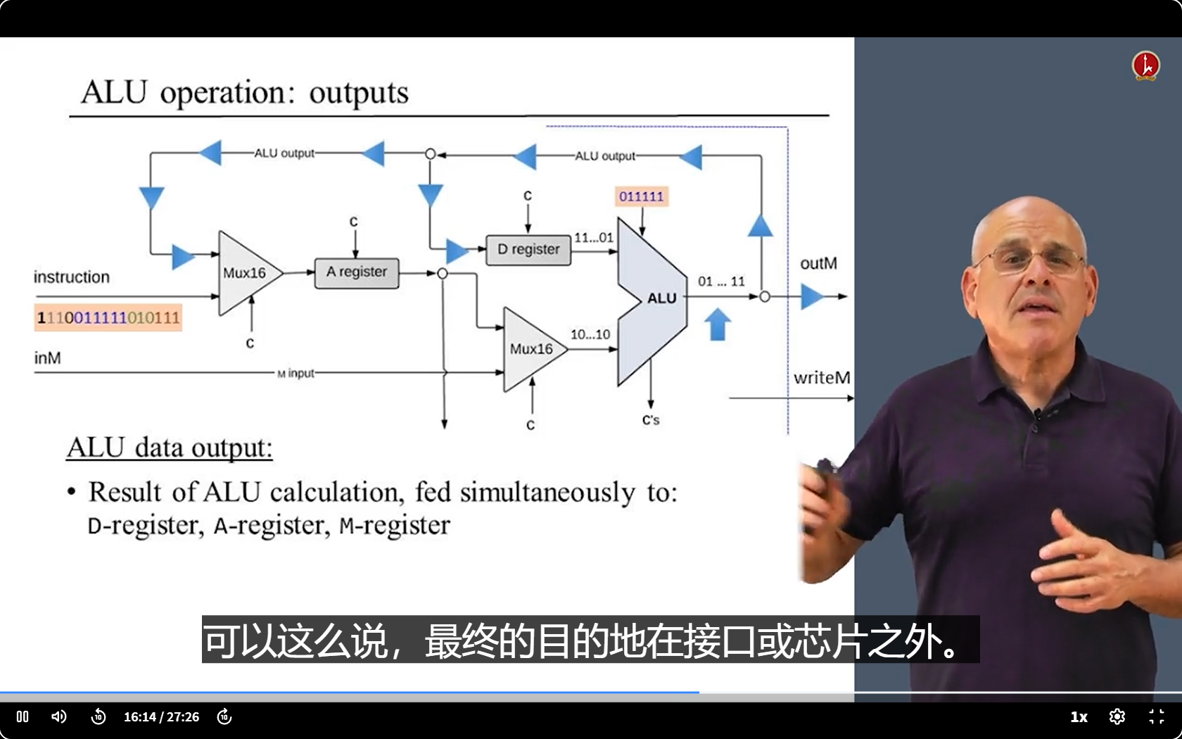
- 我们有三个目的地的位bit,这些bit决定是否打开D寄存器、A寄存器和数据存储器来接受ALU的输出。(即有选择性地接收)
Control bit c’s?
- 这两个控制位用于记录ALU的输出是负还是零。
- important for what follows.
CPU:Control (logic
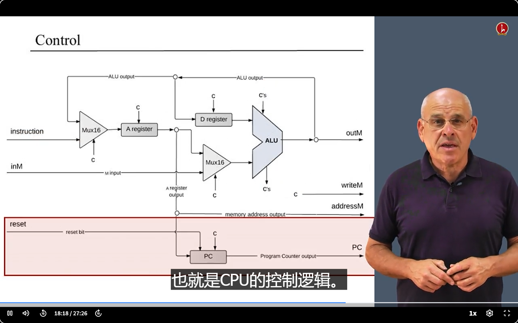
- if 程序员已经事先将想要跳转到的地址存入了A寄存器。如果我们执行PC等于A,程序计数器将输出接下来必须执行的下一条指令的地址。
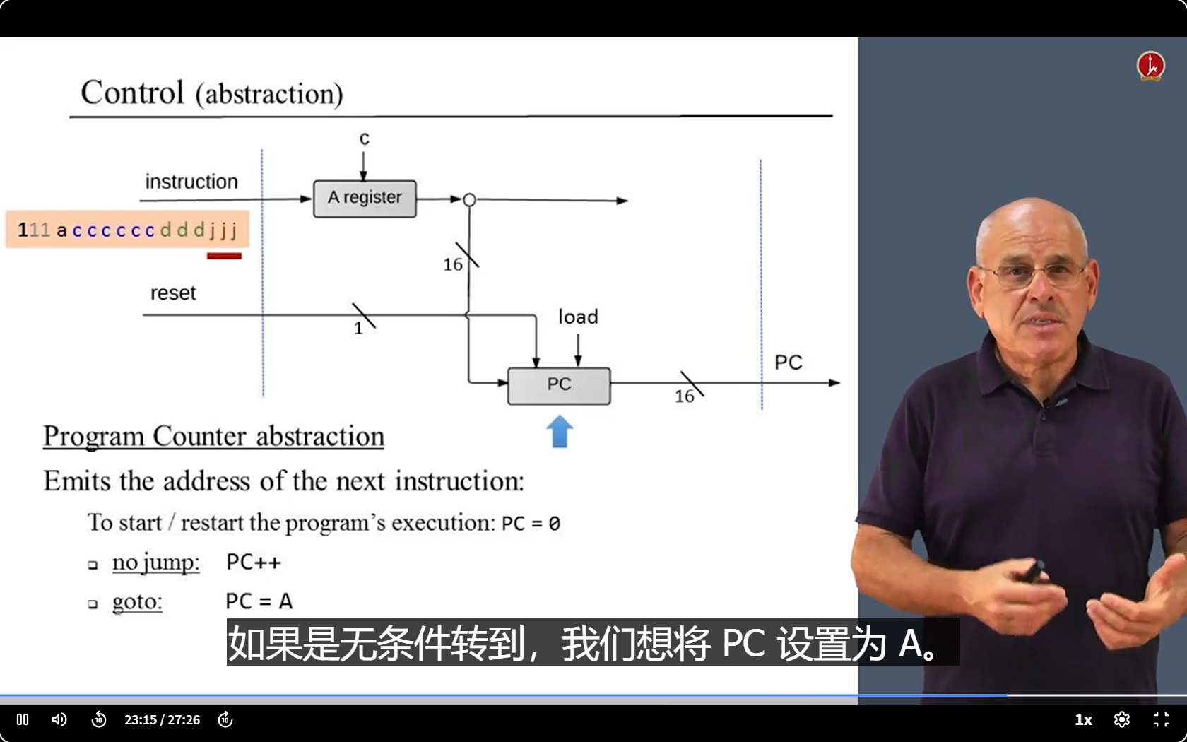
- 如果我们有一个条件跳转,我们必须查看ALU的输出,并决定这个跳转是否应该实际发生。
- 例如,假设我们有一个条件跳转指令是 “如果寄存器 A 中的值大于寄存器 B 中的值,则跳转到地址 X”。在执行这条指令之前,会先让 ALU 进行 A - B 的运算,然后根据 ALU 的输出结果(如果结果大于 0,表示 A 大于 B)来决定是否跳转到地址 X。
Last :we finish CPU
next
5.4 The Hack Computer
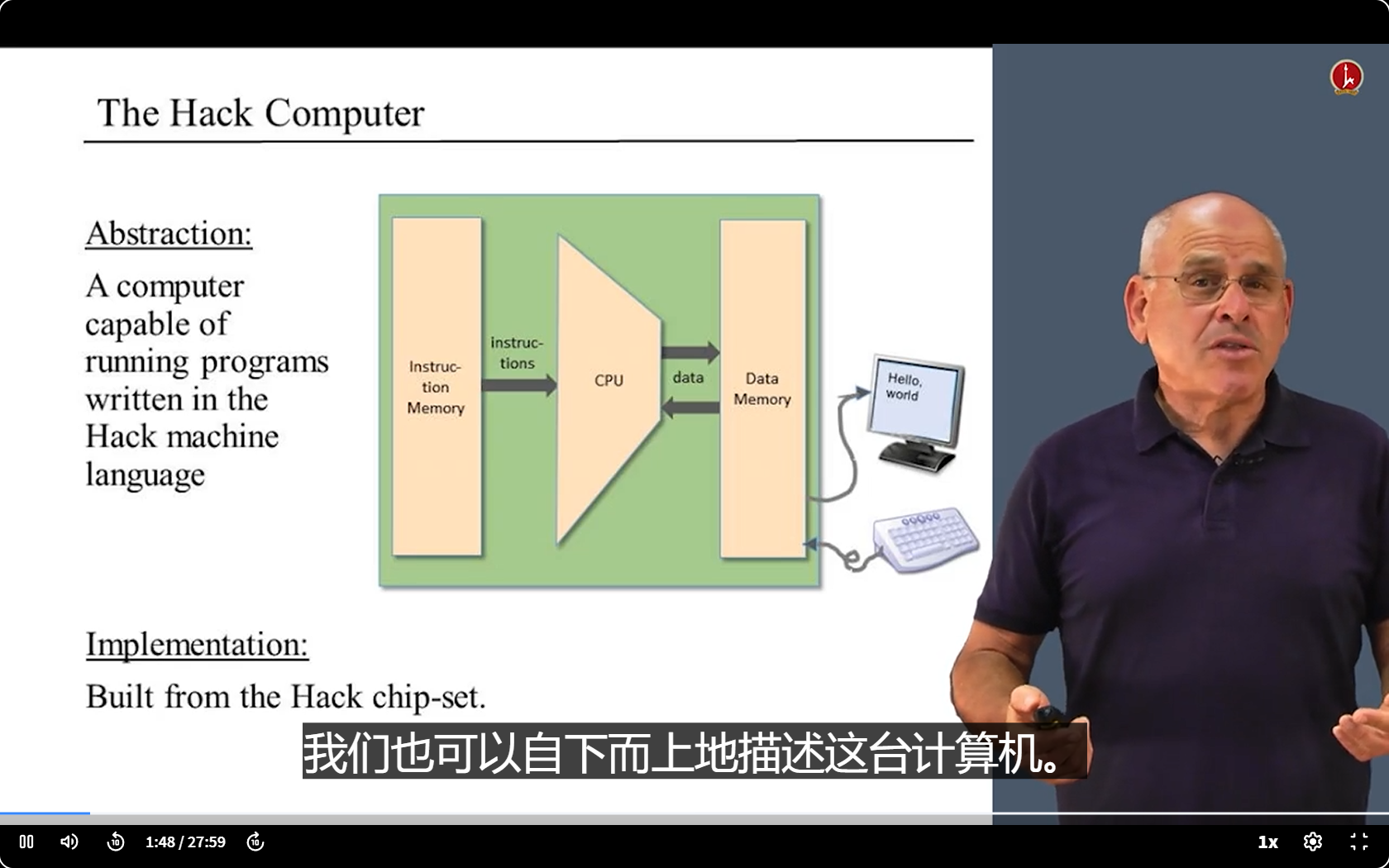
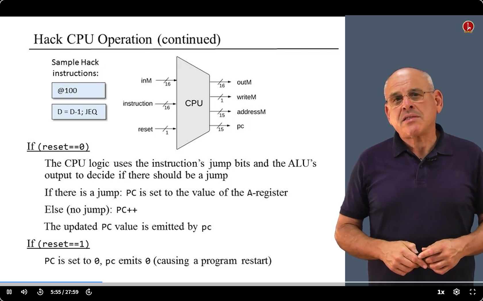
Hack CPU Operation
- 如果指令中提到了助记符“D”和“A”,CPU就会操作位于CPU内部的相应的D寄存器和A寄存器。
- 如果指令是一条A指令,在这种情况下,CPU会取出数据值,即这条指令中所谓的15位的“x”,然后将其放入A寄存器中。
- 如果指令的右侧(xxx=M)包含 “M”,这个值将从 “inM” 读取。
- 如果指令的左侧(M=xxx)包含 “M”,那么 ALU 的输出将通过 “outM” 输出,并且 “writeM” 位会→1。
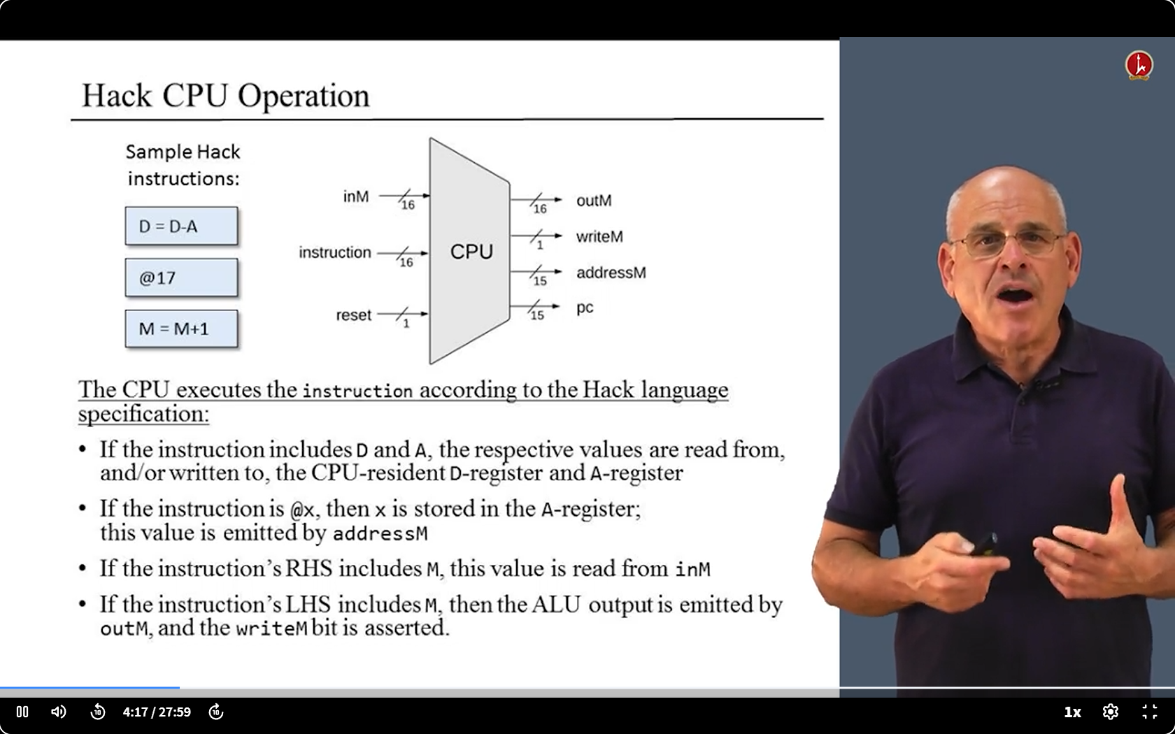
- 看看CPU如何处理跳转指令
Memory
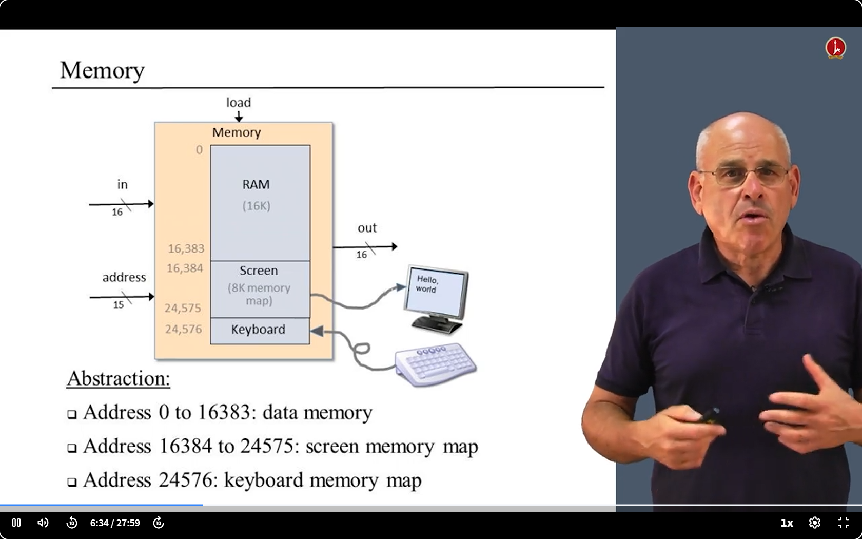

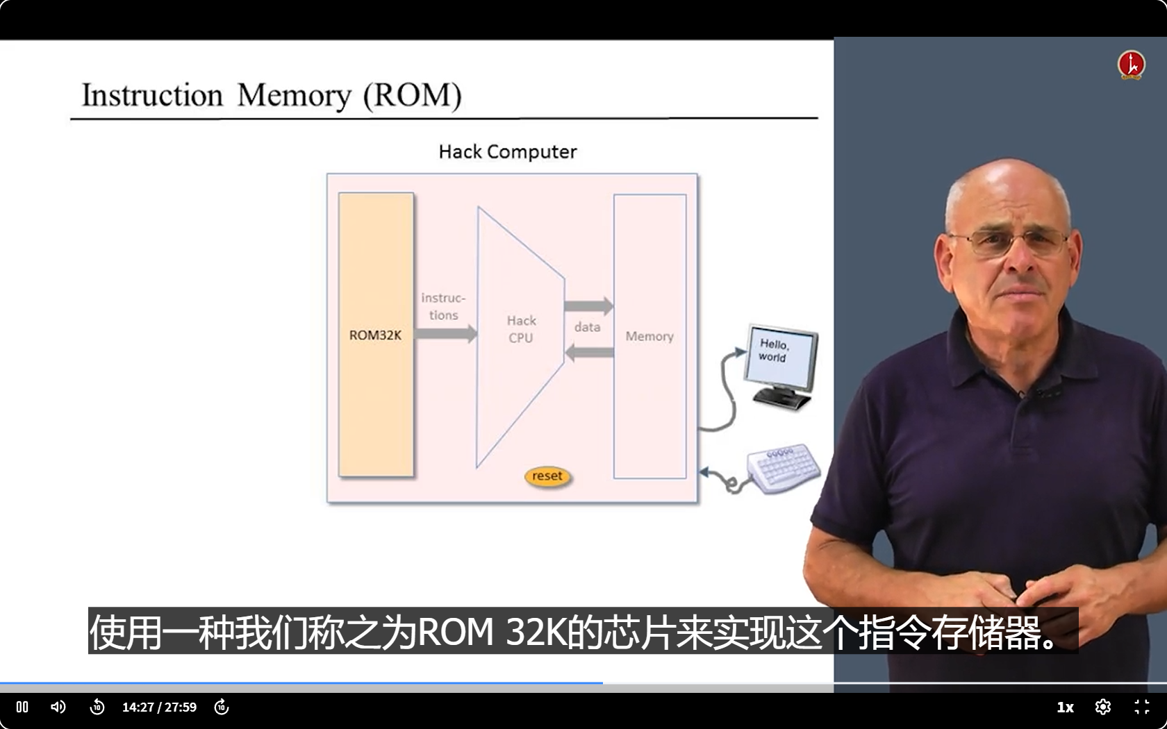
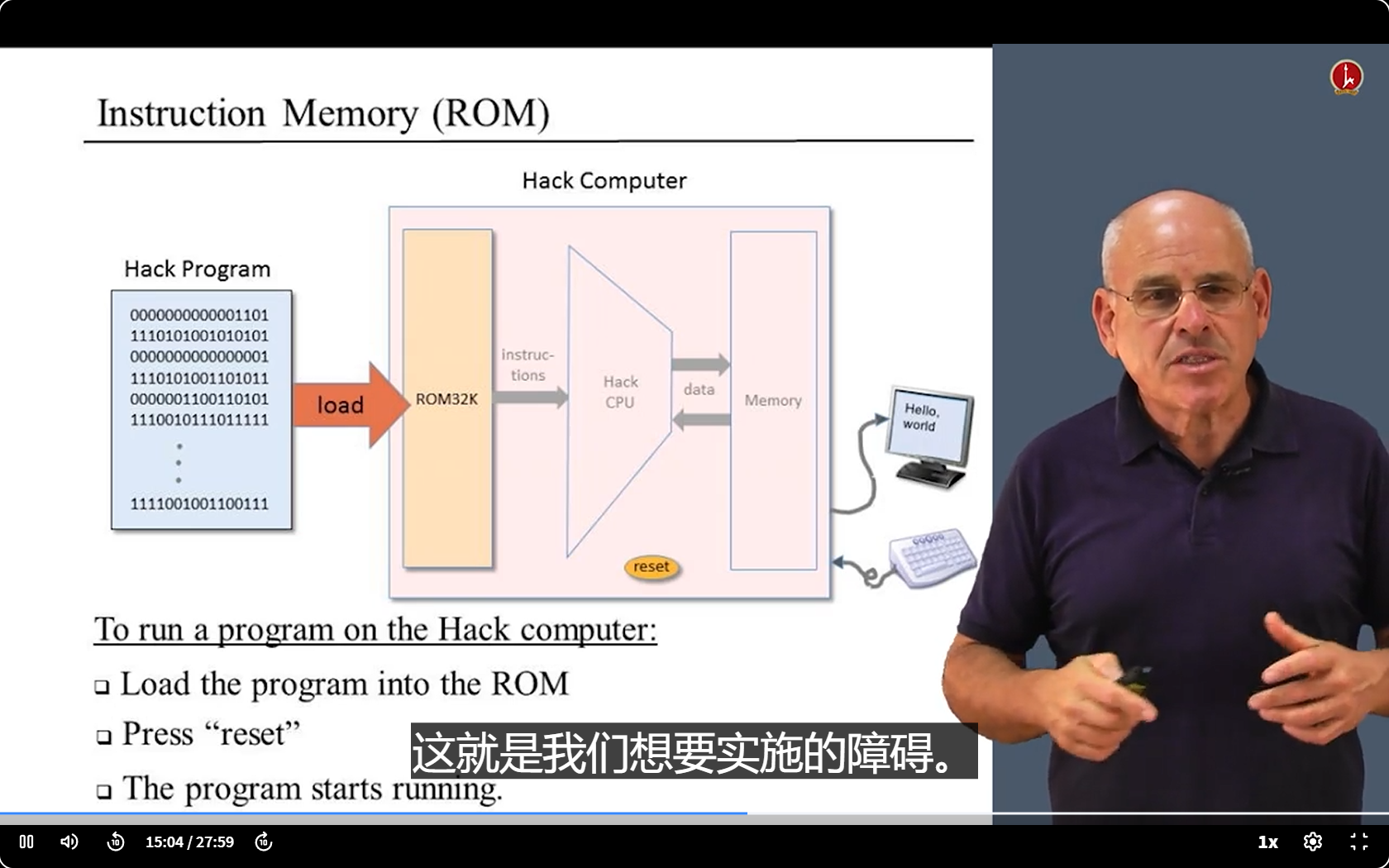
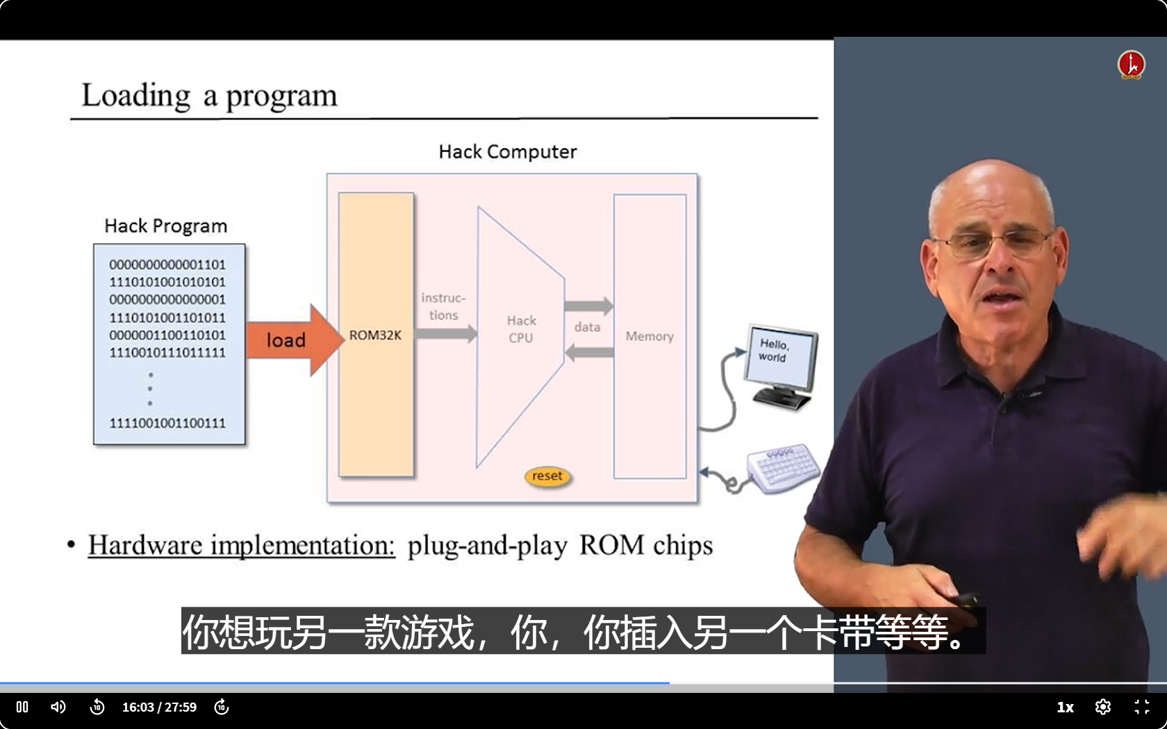
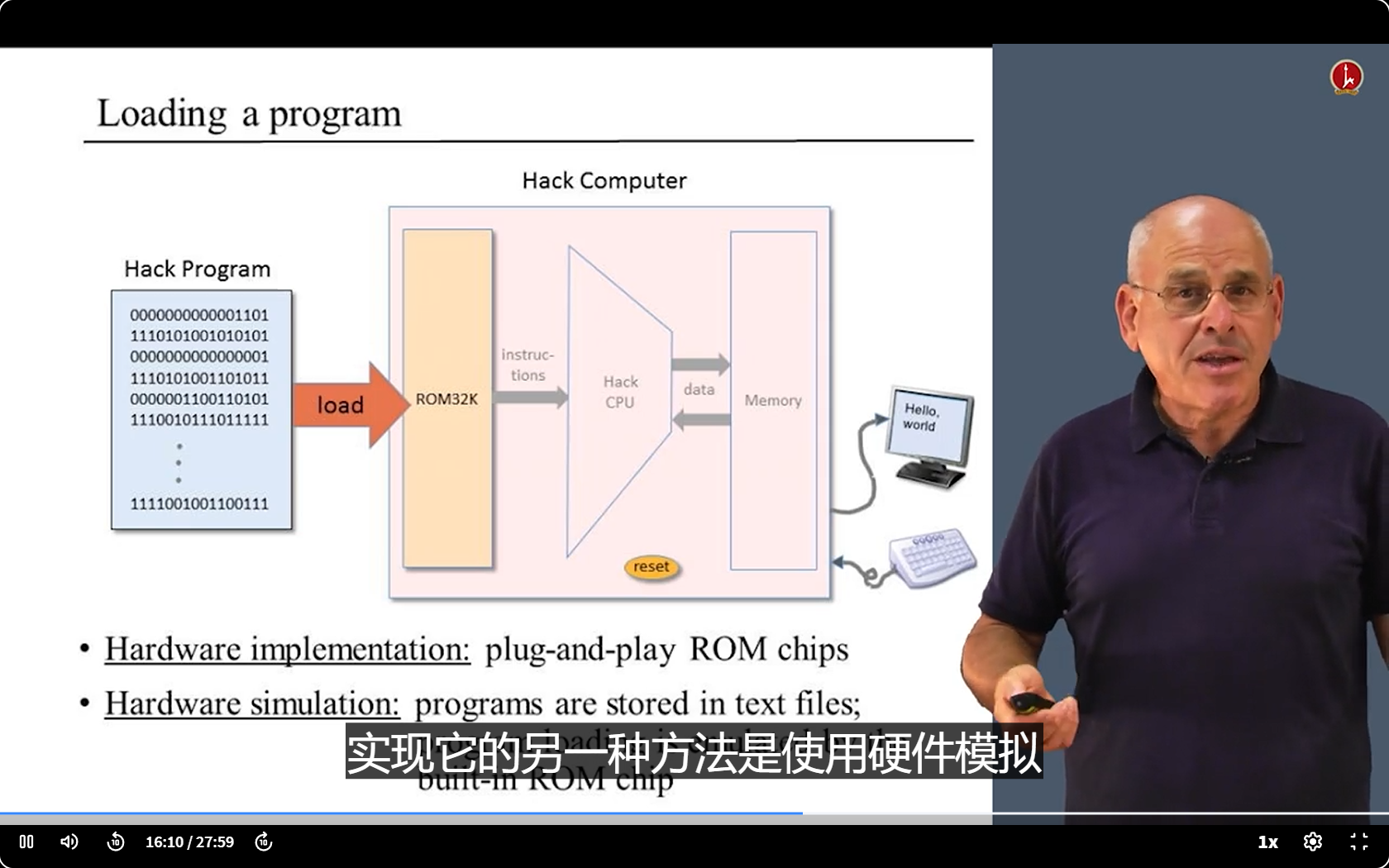
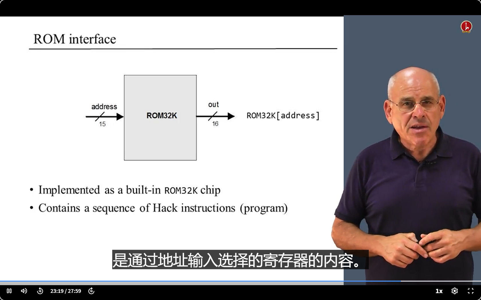
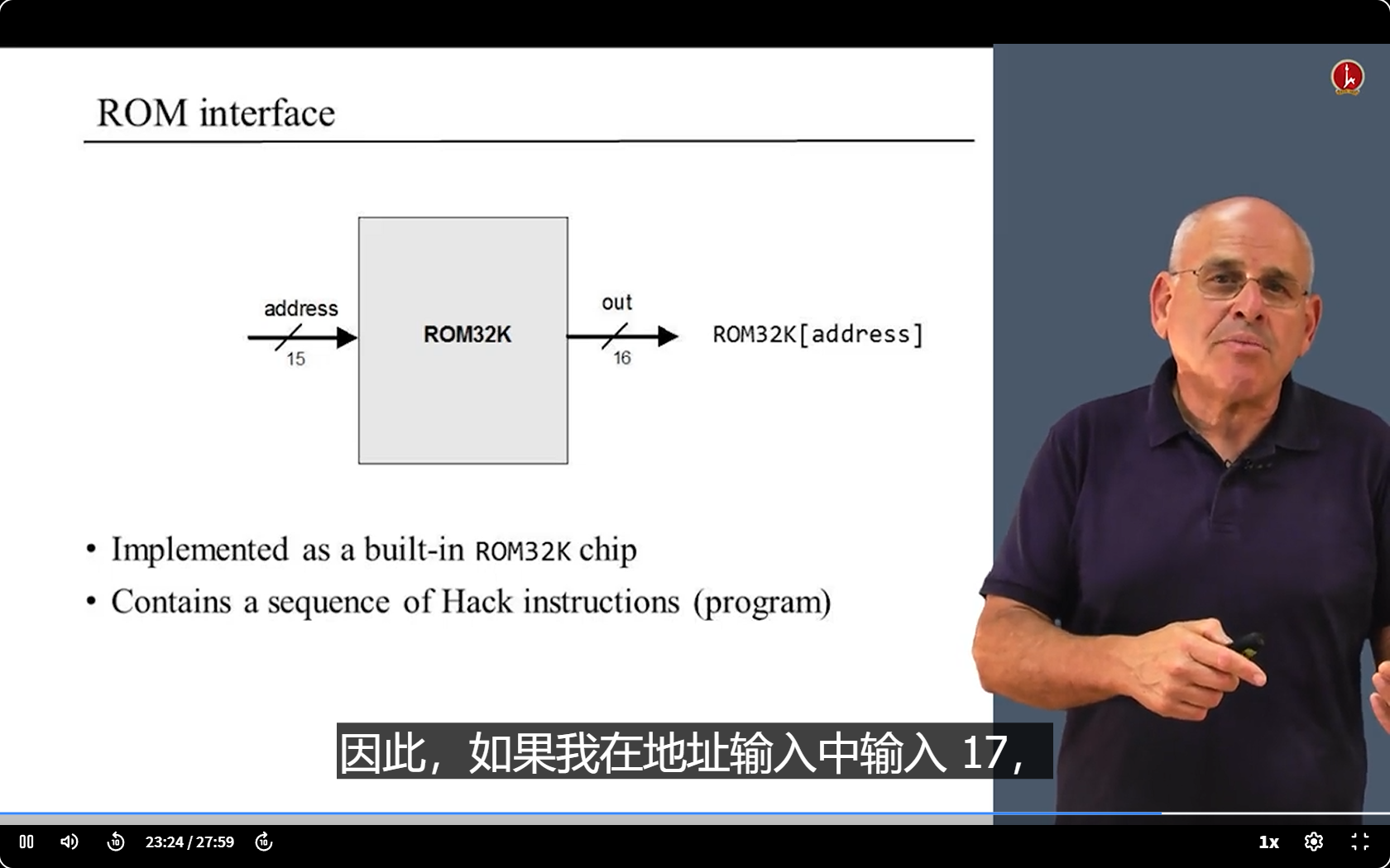
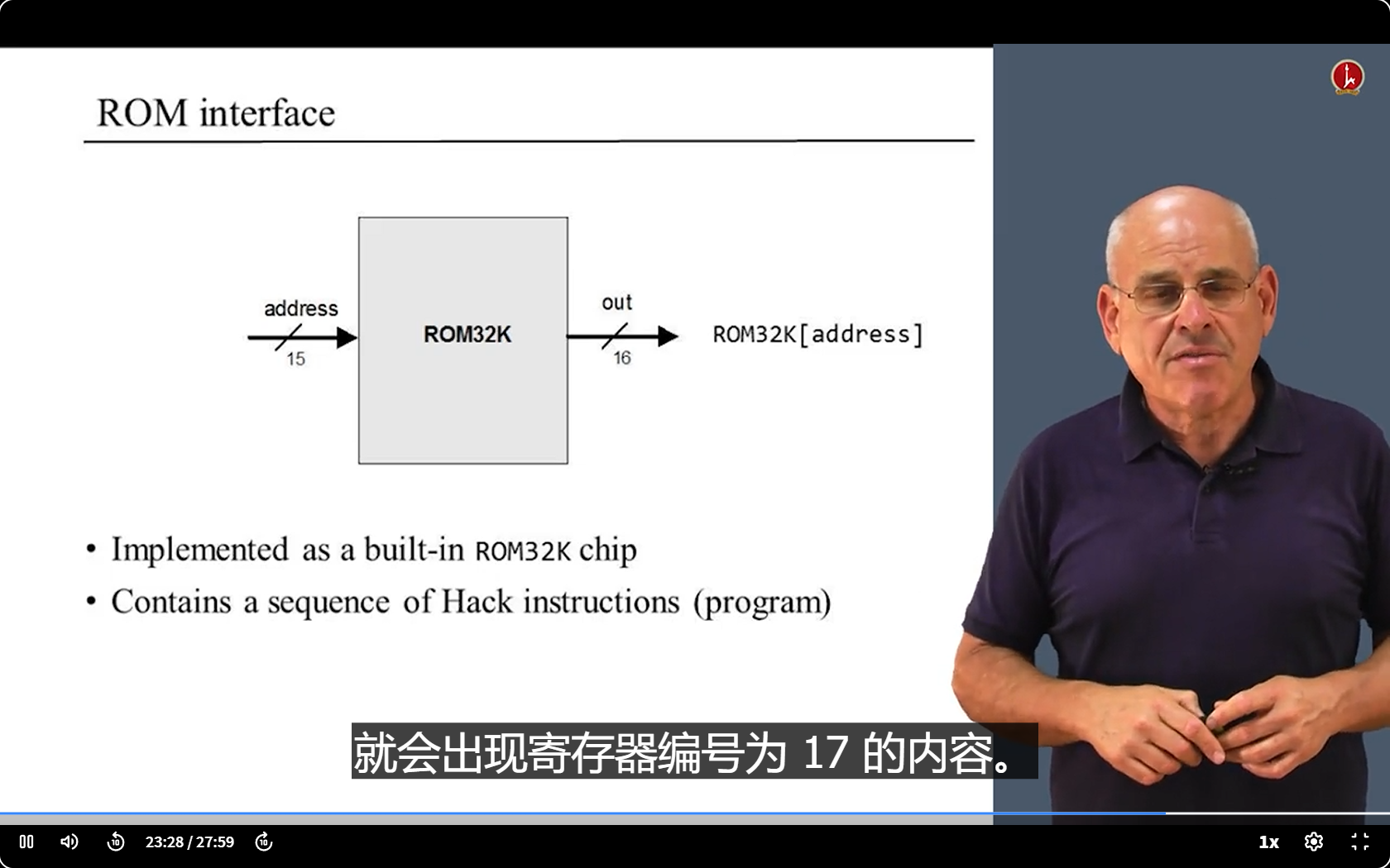
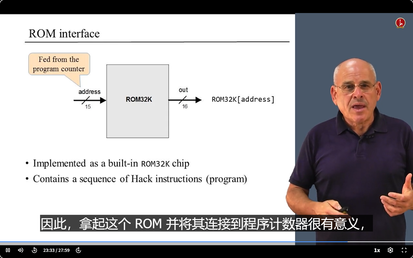
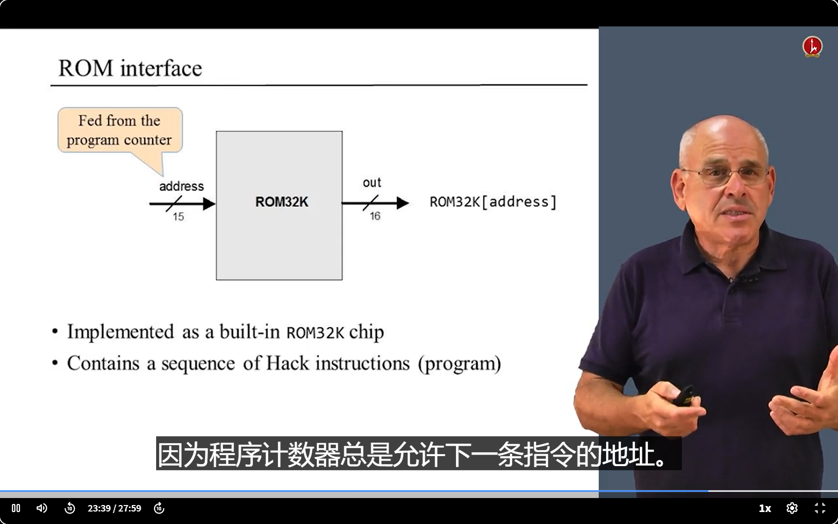
指令存储器 Instruction Memory (ROM:Read - Only Memory)
在计算机运行之前,需要将编写好的 Hack 程序数据固化到 ROM32K 芯片中。
程序中的每一条指令都按照一定的顺序和格式存储在 ROM 的不同存储单元中,每个存储单元都有唯一对应的地址。
在 Hack 计算机运行时,程序计数器(PC)会不断地向 ROM 的地址端口提供地址,ROM 根据这些地址输出相应的指令,然后 CPU 从 ROM 的输出中获取指令并执行,从而实现整个程序的运行。
- 例如,当 PC 输出地址为 0 时,ROM 会从地址为 0 的存储单元中取出对应的 Hack 指令,传递给 CPU 去执行,然后 PC 再递增,指向下一个地址,ROM 又输出下一条指令,如此循环,使得程序能够按顺序执行。

5.5 code
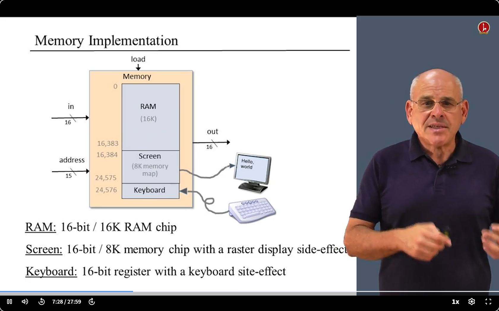
RAM16K,Screen,Keyboard
background
8K = 2的13次方。16K = 2的14次方。
address[15] 表示 address 是一个 16 位的信号。address[15] 是第 1 位,address[0] 就是第 16 位。
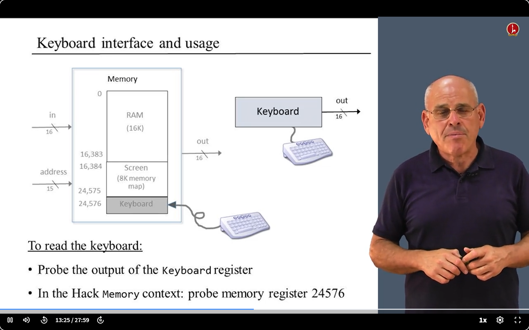
RAM16K 的地址范围:**(16K)**(0到16383)需要 14 位地址来唯一标识每个存储单元,即 address[0..13] 这 14 位地址。
Screen 的地址范围:**(8K)**(16384-24575)需要使用 13 位地址(address[0..12])就可以满足其寻址需求。
可以明显看出,一个地址如果在0-16383内,它就属于 RAM16K 的地址空间;如果在16384-24575内,它就属于 Screen 的地址空间。所以它们的地址是分开的,没有重合。
1 | CHIP RAM16K { |
1 | CHIP Screen { |
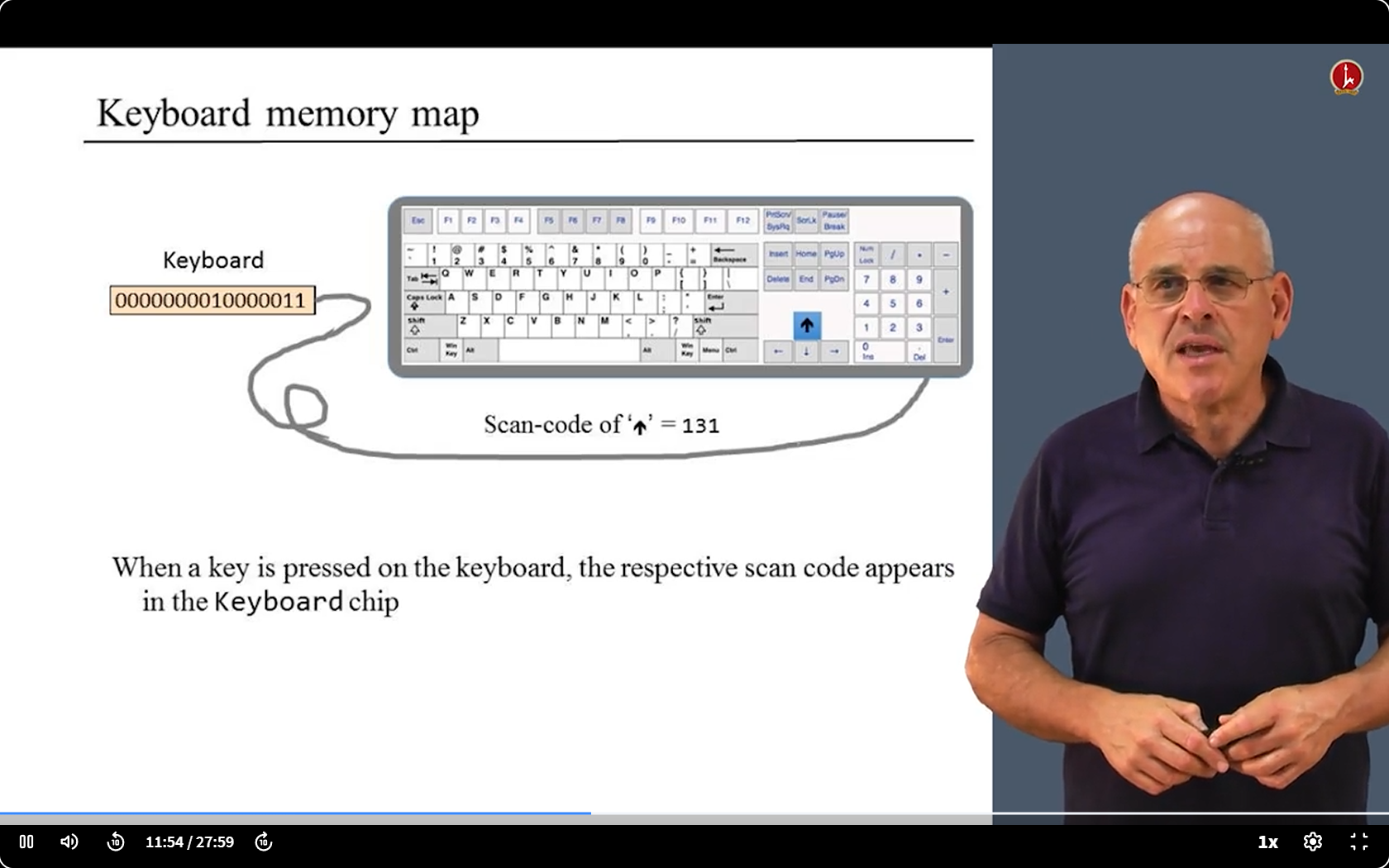
1 | CHIP Keyboard{ |
Memory
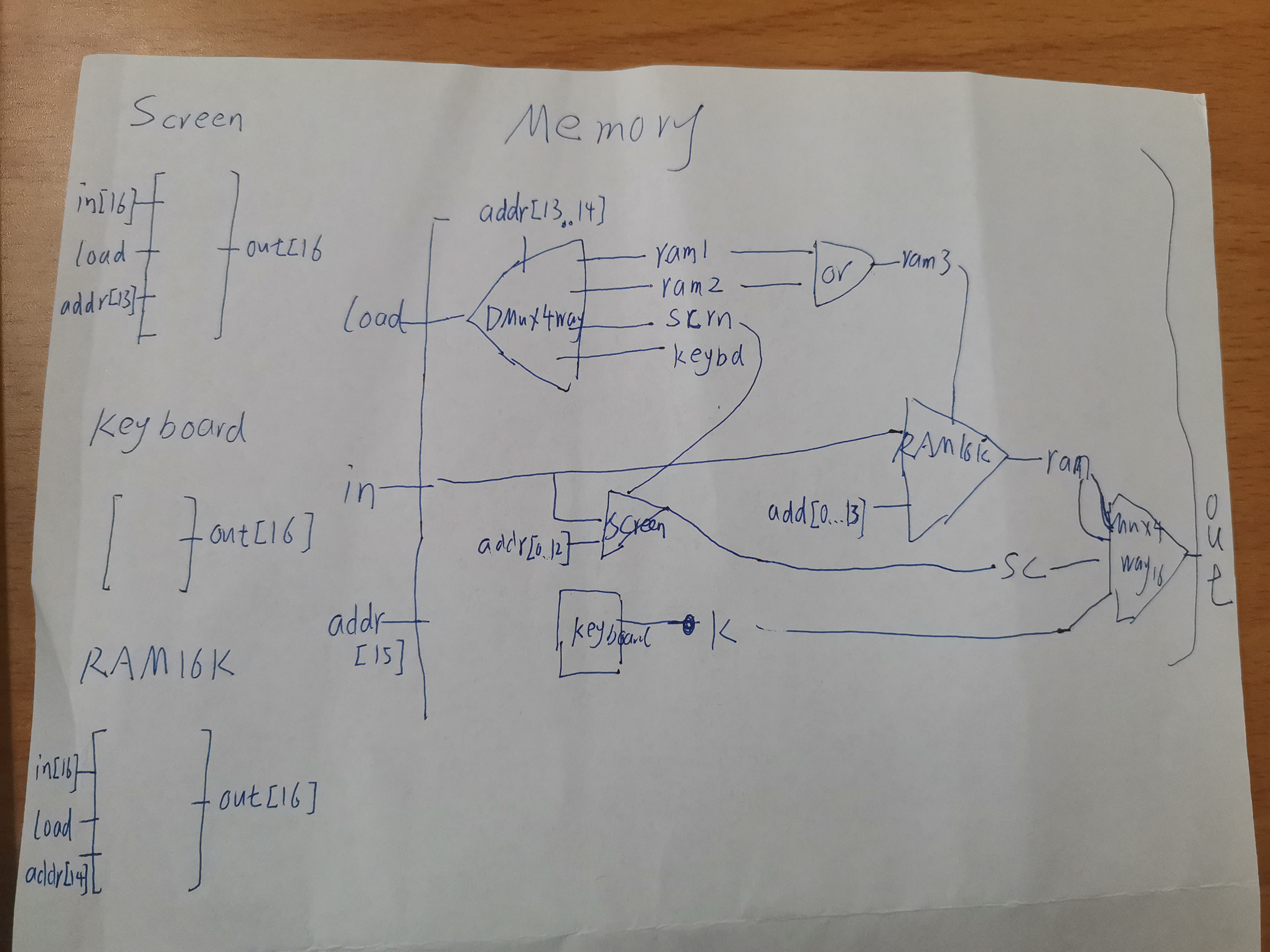
1 | CHIP Memory { |
CPU

1 | CHIP CPU { |
1 | // ALU |
Computer
1 | CHIP Computer { |